전기장 광화학 증착법에 의한 직접패턴 비정질 FeO x 박막의 제조 및 저항변화 특성
김수민·이홍섭†
강원대학교 재료공학과
Electric-field Assisted Photochemical Metal Organic Deposition for Forming-less Resistive Switching Device
Su-Min Kim and Hong-Sub Lee†
Department of Materials Science & Engineering, Kangwon National University, 1 Kangwondaehak-gil, Chuncheon-si, Gangwon-do 24341, Korea
(Received November 6, 2020: Corrected December 1, 2020: Accepted December 2, 2020)
초 록: Resistive RAM (ReRAM)은 전이금속 산화물의 저항변화 특성을 이용하는 차세대 비휘발 메모리로 전이금속 산화물 내의 산소공공의 재분포를 통한 저항변화 특성을 이용한다. 따라서 저항변화 특성을 위해 전이금속산화물 내에는 일정량 이상의 산소공공이 요구되며 이를 위해서는 박막 형성 공정에서 산화 수를 조절할 수 있는 공정이 필요하다. 본 연구에서는 직접패턴이 가능한 photochemical metal organic deposition (PMOD) 공정을 사용하여 UV 노출에 의해 photochemical metal organic precursor의 ligand가 분해되는 과정에서 전기장을 인가하여 박막내의 산화 수를 조절하는 실 험을 진행하였다. Electric field assisted PMOD (EFAPMOD) 법을 이용하여 FeO
x박막의 산화 수 조절이 가능함을 x-ray photoelectron spectroscopy (XPS) 분석과 I-V 측정을 통하여 확인하였으며, EFAPMOD 공정 중 인가하는 전압의 크기를 조절하여 박막의 산화 수를 조절할 수 있음을 확인하였다. 따라서 EFAPMOD 공정 중 인가전압의 크기를 이용하여 저항 변화 특성에 적합한 적정한 산화수를 가지는 금속산화물 박막을 얻고 그 저항변화 특성을 조정할 수 있음을 확인하였다.
Abstract: Resistive RAM (ReRAM) is a strong candidate for the next-generation nonvolatile memories which use the resistive switching characteristic of transition metal oxides. The resistive switching behaviors originate from the redistribution of oxygen vacancies inside of the oxide film by applied programming voltage. Therefore, controlling the oxygen vacancy inside transition metal oxide film is most important to obtain and control the resistive switching characteristic. In this study, we introduced an applying electric field into photochemical metal-organic deposition (PMOD) process to control the oxidation state of metal oxide thin film during the photochemical reaction by UV exposure. As a result, the surface oxidation state of FeO
xfilm could be successfully controlled by the electric field-assisted PMOD (EFAPMOD), and the controlled oxidation states were confirmed by x-ray photoelectron spectroscopy (XPS) I-V characteristic. And the resistive switching characteristics with the oxidation-state of the surface region could be controlled effectively by adjusting an electric field during EFAPMOD process.
Keywords: Iron oxide, Resistive switching, ReRAM, Photochemical metal-organic deposition, Electric field assisted
1. 서 론
Resistive RAM (ReRAM)은 외부 전압에 의해 저항변화 특성이 나타나는 전이금속 산화물을 이용하는 저항 변화 메모리로 phase change RAM (PCRAM), ferroelectric tunnel junction (FTJ), spin toque transfer magnetic RAM (STT MRAM) 등과 같이 기존 전하저장 방식이 아닌 재
료의 저항변화를 이용하는 차세대 비휘발 메모리이다.1-7) 여기서 사용되는 전이금속 산화물은 전류 또는 전기장에 의해 유도되는 산소 음이온의 electrochemical migration과 그로인한 박막 내 산화 수 변화에 의해 그 특성이 나타난 다. 산소 음이온의 electrochemical migration을 위해서는 박막내 일정량 이상의 산소공공이 필요하며 이를 위해 금 속 산화물의 산화 수 조절은 저항변화 특성을 결정하는
Corresponding author
E-mail: [email protected]
© 2020, The Korean Microelectronics and Packaging Society
This is an Open-Access article distributed under the terms of the Creative Commons Attribution Non-Commercial License(http://creativecommons.org/
licenses/by-nc/3.0) which permits unrestricted non-commercial use, distribution, and reproduction in any medium, provided the original work is
properly cited.
etching 공정없이 spin coating 후 UV 조사를 통하여 직접 패턴 된 박막을 저비용으로 쉽게 형성할 수 있는 기술로 UV를 통하여 반응을 개시하기 때문에 비교적 화학적으 로 안정한 precursor를 이용함으로써 다른 용액공정에 비 해 공정중의 습도 및 온도에 비교적 안정적이며 복잡한 산화물 박막 형성에도 쉽게 적용될 수 있다.8,9)본 연구에 서는 electric field assisted PMOD (EFAPMOD) 공정을 도 입하여 FeOx박막을 형성하는 과정에서 산화 수를 조절 하는 실험을 진행하였다.
Fig. 1은 PMOD 공정에서 UV에 의해 photochemical precursor가 개시되는 반응을 나타내는 모식도이다.
(1) (2) (1), (2)번 식은 UV조사에 의한 광화학 반응식을 나타 내며 L은 ligand를 의미한다. 본 실험에서는 광감응성 전 구체인 Fe(III) 2-ethylhexanoate를 사용하여 실험을 진행 하였다. 기판 위에 코팅된 광감응성 전구체에 UV를 조사 시키면 순차적으로 개시반응과 성장반응이 진행된다. 개 시반응은 Fig. 1(a)와 같이 Fe(III) 2-ethylhexanoate 전구체 가 광분해 되는 반응을 의미하며 분해 과정 중 생긴 유기 물들은 또다시 CO2, -C7H15로 분해 된다. 지속되는 UV 조 사과정의 생성물 Fe3+, CO2, C7H15 중 CO2는 공기중으로 확산되어 사라진다. -C7H15라디칼은 Fig. 1(b)처럼 수소
2. 실험방법
Iron oxide 박막을 형성하기 위해 UV에 의해 분해반응 이 일어나는 광감응성 precursor로 Iron(III) 2-ethylhexanoate (SigamAldrich)와 용매 n-hexane를 사용하여 0.01 mol 용 액을 제조 후 24시간동안 45oC 열에 교반기를 통해 용해 시켰다. E-beam evaporator를 이용하여 세척된 SiO2(300 nm)/p-si 기판 위에 Au 50 nm 하부전극을 형성하였으며 제작된 Fe PMOD 용액을 기판 위에 도포하여 2500 RPM 30초간 spin coating을 진행하였다. Spin coating 후 잔류 n-hexane을 제거하기 위해 hot plate 위에서 120oC, 60초 열처리를 진행하였다. Fig. 2는 실험 공정의 모식도로 표 면에 코팅된 Iron(III) 2-ethylhexanoate 박막에 UV조사와 동시에 전압을 인가하기 위해 ITO glass를 상부에 접촉하 여 UV는 투과되면서 전압이 인가될 수 있도록 하였다.
Keithley2400 source meter를 상부 ITO glass와 하부전극 에 연결한 후 Mask aligner (Pro win M-150)에서 1100초 동안 UV 노출과 동시에 전압을 각각 0 V, +5 V, + 10 V, +20 V 인가하여 50 nm 두께의 FeOx 박막을 완성하였다.
전기적 특성 평가를 위해 e-beam evaporator를 이용하여 40 nm 두께, 200 um × 200 um 면적의 Au 상부전극을 증 착하여 metal/insulator/ metal (MIM)구조의 소자를 제작하 였다.
Photochemical reaction으로 형성된 박막이 결정성을 FeL3→hv Fe+3L
Fex+O2→FexOy
Fig. 1. (a) Initiation reaction (b) Propagation reaction of Fe(III) 2-ethylhexanoate.
가지고 있는지 확인하기 위해 x-ray diffraction (XRD, PANalytical X`Pert PRO MPD)을 측정하였으며 그 결과 모든 공정조건에서 (UV 노출시 전압인가) Si 기판 피크 이외에 FeOx박막의 회절 피크는 관찰되지 않았다. 잔류 유기물 제거를 위한 120oC, 60초 열처리 외에 별도의 상 형성을 위한 고온 열처리 과정없이 상온에서 진행된 공 정으로 비정질의 FeOx 박막이 형성되었음을 확인할 수 있었다. 공정 중 전압이 인가 여부에 따라 표면의 산화 수 의 변화를 관찰하기 위해 X-ray photoelectron spectroscopy (XPS, Thermo Scientific K Alpha+)를 측정하였으며, 제작 된 MIM 구조 소자의 저항변화특성을 측정하기 위하여 Keithley2634B를 이용하였다.
3. 결과 및 고찰
Fig. 3은 전압인가 유무에 따른 FeOx 박막의 XPS 표면 분석 결과이며 Fig. 3(a), (b)는 as deposited 박막의 O 1s, Fe 2p photoelectron을 나타내고 Fig. 3(c), (d)는 전압을 인 가한 박막의 O 1s, Fe 2p photoelectron 나타낸다. 먼저 O 1s의 peak ‘a’, ‘b’, ‘c’, ‘d’, ‘e’ 는 각각 C-O, Fe-OH, Fe-O, Fe2O3, Fe3O4 결합에 의한 peak으로 binding energy는 각 각 532.05 eV, 531.1 eV, 530.5 eV, 529,9 eV, 529.2 eV이 다.10-12) 관찰된 O 1s, Fe 2p photoelectron peak을 이용하 여 atomic percent계산 결과 +10 V를 인가한 샘플의 경우 전압이 인가되지 않은 샘플에 비해 약 5% 높았으며 이는
Fig. 2. Schematic diagram of the electric field-assisted photochemical metal-organic deposition process.
Fig. 3. XPS spectrum of FeO
xfilm. (a) O 1s, (b) Fe 2p of EFAPMOD +10V film, and (c) O 1s, (d) Fe 2p of as-deposited film.
샘플의 경우 Fe 비율이 27.3% 전압을 인가하지 않은 샘 플 23.2 % 로 산화수가 더 높은 것으로 나타났다. PMOD 공정에서 UV 조사로 개시반응과 성장반응이 진행될 때 Fe3+ cation 생성되고 대기중의 산소와 결합하여 FeOx를 형성하는 과정에서 상부에 인가된 +10 V로 인하여 전압 이 인가되지 않은 박막에 비해 상대적으로 높은 산화상 태를 형성하는 것으로 예상되며, 전압의 극성을 고려하 였을 때 산소 음이온과의 정전기적 인력으로 인하여 상 부표면부에 산화수가 높은 영역이 형성됨을 예상할 수 있 다. 따라서 PMOD 공정에서 UV노출 시 전압을 인가할 경우 양이온 또는 음이온의 이동을 동반해 박막내의 산 화 수 분포를 조절할 수 있다는 것을 XPS 결과로 확인할 수 있다.
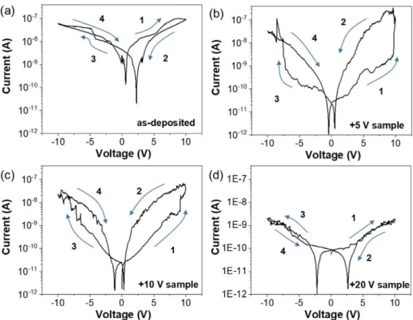
Fig. 4는 PMOD 공정 중 0 V, +5 V, +10 V, +20 V를 인 가한 FeOx샘플의 I-V 측정 결과로 파란색 화살표와 숫자 는 voltage sweep 순서를 (0 V → 10 V → 0 V → -10 V → 0 V) 나타낸다. 비교적 두꺼운 박막 두께 (50 nm)로 인하
것으로 판단된다. 전압을 인가하지 않은 박막의 경우 Fig.
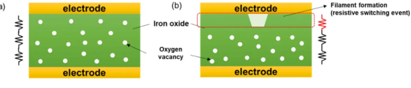
4(a)와 같이 저항이 낮고 ±10 V전압 이내에서는 저항변 화 특성이 거의 관찰되지 않았으나 PMOD 공정 중 전압 을 인가한 FeOx 박막의 경우 Fig. 4(b), (c)에서 보는 바와 같이 저항변화 특성이 관찰되었다. 이는 Fig. 5(b)와 같이 표면부에 국부적으로 산화수가 높은, 즉 저항이 높은 영 역이 존재함을 의미하며 이 경우 국부적으로 저항이 높 은 영역에서 voltage drop이 발생, 이 영역에서 filament 형 성 및 소멸에 의한 저항변화 특성이 나타난다.16,17) 그러 므로 낮은 전류양으로 (µA 이하) HRS, LRS switching이 가능한 낮은 동작전류의 저항변화소자가 형성되었다. 반 면 Fig. 4(d)의 +20 V 샘플의 경우 공정 중 높은 전압에 의해 저항 층 (산화수가 높은 FeOx)의 두께가 두껍게 형 성되어 ±10 V 전압 이내에서는 저항변화 특성이 거의 관 찰되지 않았고 매우 높은 절연특성을 나타냈다. 이는 PMOD 공정에서 UV노출 시 인가전압의 크기에 따라 표 면 부 조성의 조절이 가능함을 보여주는 결과이다.
Fig. 4. I-V characteristics of FeO
xfilms (a) as-deposited, (b) EFAPMOD +5 V, (c) EFAPMOD +10 V, (d) EFAPMOD +20 V samples.
4. 결 론
본 연구에서는 PMOD 용액공정을 이용하여 저비용의 직접패턴이 가능한 ReRAM 소자재료의 특성 조절을 위 하여 산화물 박막내의 산소농도 분포를 조절하고자 UV 조사과정에서 전압 인가장치를 도입함으로써 EFAPMOD 공정을 개발하였다. UV 조사과정에서 인가전압에 따라 산화 수 변화가 가능함을 XPS 측정을 통하여 확인하였 으며 I-V 특성측정을 통하여 인가전압의 크기가 증가함 에 따라 산화 수 또한 증가시킬 수 있음을 확인하였다.
인가전압이 높아짐에 따라 저항이 증가하였으며 UV 노 출과정에서 +5 V, +10 V가 인가된 박막은 초기저항이 HRS로 시작하여 positive voltage에서 LRS로 변화되는 counterclockwise switching curve가 관찰되었다. 표면부에 국부적으로 산화수가 높은, 즉 저항이 높은 영역이 형성 되었음을 의미하며 국부적으로 저항이 높은 영역에서 voltage drop이 발생, 이 영역에서 filament 형성 및 소멸 에 의한 저항변화 특성이 나타난다. 향후 박막 두께를 감 소시켜 동작전압을 낮추게 되면 저전력 구동이 가능하며 동시에 저항 조절이 가능한 저항변화 소자구현이 가능할 것으로 기대된다.
감사의 글
This work was supported by the National Research Foundation of Korea (NRF) grant funded by the Korea government (MSIT) (2019R1F1A1059637).
References