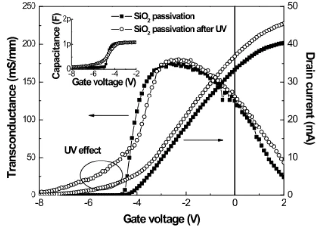
Deformation of the AlGaN/GaN metal-oxide-semiconductor heterostructure field-effect transistor characteristics by UV irradiation
6
0
0
전체 글
(2)
(3)
(4)
(5)
(6)
수치


관련 문서
Bactericidal effect of photocatalytic reactor depending on the UV-A illumination time and flow rate of V.. Bactericidal effect of photocatalytic reactor
In this regard, this study analyzes the effect of the job characteristics and work environment of workers with physical disabilities on job satisfaction
J.(2009), Characteristics of transformational leadership of nursery director child care teacher was late effect on the organization and Indications immersive
This study the changes in structure and mechanical characteristics by the analysis on mechanical characteristics of the welding part and the post weld
mould with rapid and uniform cooling characteristics using the deposition of the multi-materials based on the direct metal rapid tooling process.. In order
The purpose of this research was to identify the mediating effect of unconditional self-acceptance and the moderated mediating effect of emotional
This study examined the mediating effect of Executive Function in The Effect of Mother’s Play Participation in Child’s Emotion Regulation.. The participants
Activated H-Ras expression in human fibroblast cell lines increases the activity of Ku80 to bind injuried DNA, reduces γ-H2AX expression by UV irradiation,
