The Effect of Thermal Concentration in Thermal Chips
Kyo Sung Choo † · Il Young Han * · Sung Jin Kim **
Key Words :
Diode Temperature Sensor Array(다이오드 온도센서), Hot Spot(핫 스팟), Wafer Thinning(웨이퍼 박판화)Abstract
Hot spots on thin wafers of IC packages are becoming important issues in thermal and electrical engineering fields.
To investigate these hot spots, we developed a Diode Temperature Sensor Array (DTSA) that consists of an array of 32 x 32 diodes (1,024 diodes) in a 8 mm x 8 mm surface area. To know specifically the hot spot temperature which is affected by the chip thickness and a generated power, we made the DTSA chips, which have 21.5 µm, 31 µm, 42 µm, 100 µm, 200 µm, and 400 µm thickness using the CMP process. And we conducted the experiment using various heater power conditions (0.2 W, 0.3 W, 0.4 W, 0.5 W). In order to validate experimental results, we performed a numerical simulation. Errors between experimental results and numerical data are less than 4%. Finally, we proposed a correlation for the hot spot temperature as a function of the generated power and the wafer thickness based on the results of the experiment. This correlation can give an easy estimate of the hot spot temperature for flip chip packaging when the wafer thickness and the generated power are given.
1. Introduction
Heat dissipation is an important technology in today’s semiconductor world. In order to reduce chip size, the 3- D chip stack technique is growing rapidly using wafer thinning process [1-5]. However, the heat spreading effect is reduced in wafers because the wafer thickness has been reduced. In other words, the thermal runaway problem of chips will occur due to the effect of the hot spots, which are caused by heat concentration in the chip.
Many companies made limitations on the hot spot temperature in chips to protect the chips from the thermal runaway problem. For example, Some companies report that when two logic devices with an operating temperature limit of 125ºC and memory devices with an operating temperature limit of 100ºC are mounted together, the package’s thermal dissipation must be kept below 100ºC [6]. Thus, the thermal issues must be considered at the time of the die selection and design.
We could not, until recently, expect to see the hottest temperature on a chip at a given generated power and chip thickness since there is no correlation for the hot spot temperature as a function of the chip thickness and the generated power. Therefore, in order to know the
effect of the hot spot temperature on the chip for the various chip thicknesses, we developed a Diode Temperature Sensor Array (DTSA) that consists of an array of 32 x 32 diodes (1,024 diodes) in a 8 mm x 8 mm surface area [7]. To know specifically the hot spot temperature which is affected by the chip thickness and the generated power, we conducted the experiment using various heater power conditions (0.2 W, 0.3 W, 0.4 W, 0.5 W). In order to validate experimental results, we performed a numerical simulation.
Finally we obtained a simple correlation for the hot spot temperature as a function of the generated power and the chip thickness. Therefore we can avoid the thermal runaway problem on the semiconductor chips of a flip-chip design by using this correlation.
2. The design and fabrication of DTSA
2.1 Layout Design and Fabrication
It is well known that constant current causes a forward voltage drop across a silicon diode, which decreases as the temperature of the silicon diode increases. The voltage drop across the silicon diode is approximately proportional to the inverse of the absolute temperature of the diode for a wider range of temperatures [8].
To fabricate the DTSA, the DTSA was designed as shown in Fig. 1. The manufacturing process of the DTSA is as follows. First, a series of n-wells are created on a wafer. Secondly, n+ and p+ doping are diffused for the creation of p+ and n+ regions.
† Korea Advanced Institute of Science and Technology E-mail : [email protected]
TEL : (042)869-3083 FAX : (042)869-8207
* Korea Advanced Institute of Science and Technology
** Korea Advanced Institute of Science and Technology
2449
Fig. 1 Schematic of a single diode in a DTSA
Thirdly, metal1 and metal2 are deposited on the wafer for interconnecting rows and columns diodes, respectively. Fourthly, polysilicon heaters are deposited for heating and controlling the temperature of the DTSA.
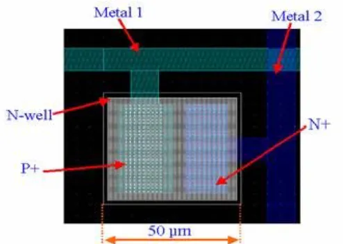
To make the DTSA masks, we designed the layout of the DTSA by using a commercial layout design program (Cadence). The size of a single diode is 50 µm x 50 µm.
By combining and rearranging the single diode layout, as illustrated in Fig. 1, an array of 32 x 32 diodes is fabricated. We refer to this array as a DTSA (Diode Temperature Sensor Array). The DTSA has 1,024 diodes in a 12 mm x 12 mm chip area. Therefore, the effective sensing area of the DTSA is 8mm x 8mm. Three metal layers are used for interconnecting the diodes and heaters in order to establish an easy connection line. The first metal layer is used only for interconnecting the n+
doping parts of each diode with the row side pads of the DTSA. The second layer is used only for interconnecting the p+ doping parts of each diode with the column side pads. Lastly, the third metal is used for interconnecting the polysilicon heaters with the heater pads of the DTSA.
3. Results and Discussion
3.1 Thermal effect of the DTSA chip thickness Normally, silicon wafer has large axial (parallel to the chip surface) conduction of heat in their chip (due to large thermal conductivity of Si wafer). If we plane chips by using CMP process to stack on the chips, however, the effect of the hot spot temperature on the chips significantly increases due to suppression of the axial heat spreading. In order to reduce the thermal damage in chips due to the hot spots, therefore, it is important to estimate the hot spot temperature as the chip thickness decreases. In this work, we investigated the effect of the hot spot temperature by using the various thicknesses of the DTSA chip.
Fig. 2 Three dimensional view of temperature distributions of the 400 µm thickness DTSA and 3 1µm thickness DTSA
Originally, chips are manufactured with a 400 µm thickness silicon wafer. As the industry continues to move ahead a greater number of chips per package and thinner chip to meet package height demands, wafer thinning and stack techniques are becoming important.
There are many methods of reducing chip thickness, until recently, however the chip cannot be easily managed for packaging to interconnect the pads of the chip to the pads of PCB because of its weakness and fragility.
We developed a simple method of minimizing the thickness of the DTSA chip. First, the DTSA is mounted with a packaging PCB by using a flip chip package, as explained earlier. The thickness of the DTSA is then reduced using a CMP (Chemical Mechanical Planarization of Semiconductor) process. The flip chip package firmly attaches the DTSA chip and the PCB with each other. The backside of the DTSA chip can then be safely removed by the CMP process. Using the CMP process, we made DTSA chips that have 21.5 µm, 31 µm, 42 µm, 100 µm, 200 µm, and 400 µm thickness.
Fig. 2 shows the temperature distributions on the DTSA surface when 0.32W is applied to the center heater embedded in the DTSA chip under 25ºC ambient temperature. The DTSA of 31 µm thickness displays a sharp cone shape temperature profile, because conduction along the chip surface is suppressed by its narrow thickness compared with the DTSA chips of 400 m thickness. To know specifically the thermal trend of the effect of the chip thickness, we conducted the various experiment using various thicknesses of the DTSA chips (21.5 µm, 31 µm, 42 µm, 100 µm, 200 µm, and 400 µm thickness) and various heater power conditions (0.2 W, 0.3 W, 0.4 W, 0.5 W)..
3.2 Numerical Analysis
In order to validate experimental results, we used a similar thermal model for the real sensor design with
2450
Fig. 3 Schematic diagram of the DTSA
ICEPAK program. Fig. 3 shows a schematic diagram for the DTSA package. Conditions of the numerical model were like as follows, system size; 50 mm x 50 mm x 2.7 mm, PCB thickness; 2 mm, underfill thickness; 0.3 mm, chip thickness 21.5 µm, 31 µm, 42 µm, 100 µm, 200 µm, and 400 µm, solder balls; 0.3 mm x 80 ea, heater size; 1 mm x 1 mm, copper line; 0.1 mm x 15 mm. The solder balls are designed hexahedron block to simplify the numerical model. Total 80 Copper lines are designed 4 directions each has 20 lines. We defined the thermal conductivity of the chip as a function of temperature [9].
The thermal conductivity of the underfill, the solders, the copper line and the PCB can be used in [10]. Also, we used the typical free convection coefficient on the sensor and PCB surfaces.
Comparative plots of simulated and measured temperature distributions are shown in Fig. 4. Errors between the calculated results and the experimental data are less than 4 %. Numerical simulation results describe bell shape for temperature distribution like as experimental results. As the chip thickness gradually decreases, the center temperature on the chip surface increased since the lateral conduction effect decreases in the chip. This package has two dominant heat transfer paths, one of which is the conduction from the solders to the board and the convection from the top of the chip to the ambient. The secondary heat transfer path is negligible as the chip thickness is thick, since the conduction effect is much larger than the convection effect. But as the chip thickness gradually decreases, the free convection effect on the chip surface becomes more important. Heat is concentrated on the center of the chip at a thickness of 21.5 µm, but heat is well dissipated from the heater to the solders by the conduction dominant effect at a thickness 200 µm. Other paths from the underfill to the board are negligible due to the low conductivity of the underfill. Likewise, other heat transfer paths from either the top or bottom of the PCB to the ambient are negligible due to the low conductivity of the PCB.
3.3 A correlation for hot spot temperature s
As mentioned in the introduction, there are thermal management problems with chip fabrication since a proper correlation for the hot spot temperature did not
2.2x10⁻² 2.4x10⁻² 2.6x10⁻² 2.8x10⁻² 30
40 50 60 70 80 90 100
110 0.3W
Exp.
20um 40um 100um 400um Num.
20um 40um 100um 400um
T e m p er at u re [
oC]
X [m]
Fig. 4 Comparative plots of temperature distribution, numerical data and experimental data
0 50 100 150 200 250 300 350 400
40 60 80 100 120 140
160
0.2W
0.3W 0.4W 0.5W correlation 0.2W correlation 0.3W correlation 0.4W correlation 0.5W
Ce nter T e mpe ra tu re [
oC]
Thickness [um]
Fig. 5 Maximum temperature variation versus the thicknesses of the DTSA
exist, until recently. Therefore, we presented a correlation to give the limits of the chip thickness. Fig. 5 presents the experimental results showing the relationship between the chip thickness and the maximum temperature. As observed, the hot spot temperature is rapidly increased as a chip thickness drops below 100 µm. From Fig. 5, we obtained a simple correlation for the hot spot temperature, the generated power, and the thickness of the chip.
max 60 290 exp
T T P 36 δ
∞
⎡ ⎛ ⎞ ⎤
= + ⎢ ⎣ + ⎜ ⎝ − ⎟ ⎠ ⎥ ⎦
(1)
Where P is the generated power and δ is the chip thickness. This correlation can estimate the hot spot temperatures within 4 % of relative errors, under the condition that the chip thickness is less than 100 µm. The hot spot temperatures for chip thicknesses of 200 µm and 400 µm are not considered since they are very small. We used the first order exponent function since we focused on the hot spot effect as the chip thickness is thin. Also
2451
the first order exponent function is mathematically simple and easy to apply the industry field. The correlation is useful since the thickness of the stacked chips of a flip-chip design in 3-D technique is usually less than 50 µm. As shown in Eq. (1), the thermal thickness effect constant is a fixed value 36. The constant is independent of the generated power and has a physical meaning. As can be seen from Fig. 5, if the designed chip thickness is less than 36 µm, the hot spot temperature is drastically increased, causing thermal runaway of the chips designed by a flip chip packaging method.
Therefore, we have to consider the appropriate chip thickness to avoid thermal problems caused by the hot spot. Namely, we can use the above equation to easily determine thermally safe chip thicknesses.
4. Conclusion
Hot spots on thin wafers of IC packages are becoming important issues in thermal and electrical engineering fields. Thermal runaway of chips will occur due to the hot spot temperature. To investigate these hot spots, we developed a Diode Temperature Sensor Array (DTSA) that consists of an array of 32 x 32 diodes (1,024 diodes) in a 8 mm x 8 mm surface area. To know specifically the hot spot temperature which is affected by the chip thickness and the generated power, we made the DTSA chips, which have 21.5 µm, 31 µm, 42 µm, 100 µm, 200 µm, and 400 µm thickness using the CMP process. And we conducted the experiments using various heater power conditions (0.2 W, 0.3 W, 0.4 W, 0.5 W). We performed a numerical simulation to validate experimental results. Errors between experimental results and numerical data are less than 4%. Finally we obtained a simple correlation for the hot spot temperature as a function of the generated power and the chip thickness.
We can avoid the thermal runaway problem of the semiconductor chips of a flip-chip design by using the correlation.
Acknowledgement
This work was supported by the Korea Science &
Engineering Foundation through the NRL Program (grant 2006-02147).
Reference
(1) Savastiouk S, Siniaguine O, and Diorio M, 1998,
"Moore’s law: the next dimension," Advances in Electronic Packaging, Vol. 7, pp. 55-58.
(2) Grief MK and Steele Jr JA, 1996, "Warpage and mechanical strength studies of ultra thin 150 mm wafers," In: IEEE/CPMT international manufacturing technology symposium, pp. 190–194.
(3) Landesberger C, Klink G, Schwinn G, and Aschenbrenner R, 2001, “New dicing and thinning concept improves mechanical reliability of ultra thin silicon,” International symposium on advanced packaging materials, pp. 92–97.
(4) Robert Wieland, Detlef Bonfert, Armin Klumpp, Reinhard Merkel, Lars Nebrich, Josef Weber, and Peter Ramm, 2005, “3D integration of CMOS transistors with ICV-SLID technology,” Microelectronic Engineering, vol. 82, pp. 529-533.
(5) Wu L, Chan J and Hsiao CS, 2003, “Cost- performance wafer thinning technology,” Electronic components and technology conference, pp. 1463–1467.
(6) A. Takashima, 2005, “The requisite technologies for SiP development,” Denshi Zairyo, pp. 23-27.
(7) I.Y.Han and S.J.Kim, 2005, “Technique for measuring and controlling micro scale surface temperature,” The Sixth KSME-JSME Thermal and Fluids Engineering Conference.
(8) A. S. Sedra and K. C. Smith, 1998,
“Microelectronic circuits,” New York: Oxford U. Press,.
(9) Frank P. Incropera and David P. DeWitt, 2002,
“Introduction to heat transfer,” New York: Wiley.
(10) W.S.Lee, I.Y.Han, Jin Yu, S.J.Kim, and T.Y.Lee, 2004, “Thermal characterization of thermally conductive underfill for a flip-chip package using novel temperature sensing technique,” Proceedings of 6th Electronic Packaging Technology Conference (EPTC), p. 47.
2452