논문 2013-50-10-8
록 시간을 줄이기 위한 변형 위상 주파수 검출기를 가진 DPLL
( A DPLL with a Modified Phase Frequency Detector to Reduce Lock Time )
하산 타릭*, 최 광 석***
( Md. Tariq Hasan and GoangSeog Choi
ⓒ)
요 약
130nm CMOS 공정 라이브러리를 이용하여 125MHz로 동작하는 새로운 위상 주파수 검출기 기반 DPLL을 설계하였다. 이 DPLL은 중간 주파수대 응용을 위해 지터와 록 시간을 줄이려고 전형적인 DPLL에 반전 에지 검출기를 포함하고 있다. XOR 기반 반전 에지 검출기들은 출력을 보다 빨리 변화시키기 위하여 기준 신호보다 빠른 전이를 얻는데 사용된다. HSPICE 시뮬 레이터는 모의실험을 위해 Cadence환경에서 사용되었다. 제안된 위상 주파수 검출기를 가진 DPLL의 성능은 종래의 위상 주 파수 검출기를 가진 것의 성능과 비교하였다. 종래의 PLL은 약 0.1245 ns의 최대 지터를 가지고 록 하는데 최소 2.144 µs가 걸린 반면에, 제안한 검출기를 가진 PLL은 약 0.1142 ns의 최대 지터를 가지고 록 하는데 0.304 µs가 걸린다.
Abstract
A new phase frequency detector based digital phase-locked loop (PLL) of 125 MHz was designed using the 130 nm CMOS technology library consisting of inverting edge detectors along with a typical digital phase-locked loop to reduce the lock time and jitter for mid-frequency applications. XOR based inverting edge detectors were used to obtain a transition earlier than the reference signal to change the output more quickly. The HSPICE simulator was used in a Cadence environment for simulation.
The performance of the digital phase-locked loops with the proposed phase frequency detector was compared with that of conventional phase frequency detector. The PLL with the proposed detector took 0.304 µs to lock with a maximum jitter of approximately 0.1142 ns, whereas the conventional PLL took a minimum of 2.144 µs to lock with a maximum jitter of approximately 0.1245 ns.
Keywords: Phase-locked loop, Lock Time, Phase Frequency Detector, Voltage Controlled Oscillator, Jitter
Ⅰ. Introduction
A digital phase-locked loop (DPLL) is a negative feedback control system, where the output frequency tracks the input frequency and rising edges of the
* 학생회원, ** 평생회원, 조선대학교 정보통신공학과 (Dept. of Info. and Comm. Eng., Chosun Univ.)
ⓒ Corresponding Author(E-mail: [email protected])
※ 본 논문은 미래창조과학부 지원으로 수행한 ETRI SW-SoC 융합 R&BD센터의 연구결과입니다.
접수일자: 2013년6월10일, 수정완료일: 2013년9월27일
output data clock (dclk) align to the rising edges of the reference input signal (data). A DPLL plays an important role in communication and digital systems for frequency synthesis, skew cancellation, demodulation, clock recovery etc. Usually there are two types of DPLL based on the type of detector.
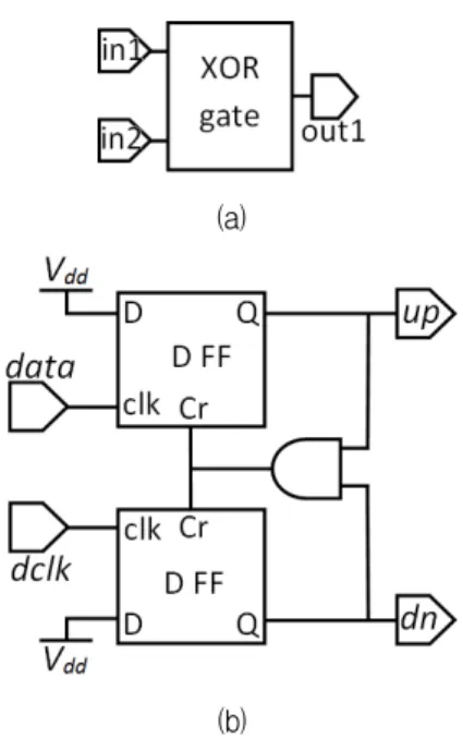
One having XOR based phase detector (PD) and another one having D flip-flop based phase frequency
detector (PFD), as shown in Figure 1. XOR based
PD has some inherent drawbacks for the application(a)
(b)
그림 1. DPLL (a) 위상 검출기 (b) 위상 주파수 검출기 Fig. 1. Unit of a DPLL (a) phase detector (b) phase
frequency detector.
in DPLL. These are- it can lock on harmonics of input reference signal, the width of the input reference signal and DPLL output signal is very much important in taking phase information from PD, and it uses only phase information, that is, it does not deal with the frequency information. On the contrary, D flip-flop based PFD is free from all these drawbacks and mostly used but it has poor noise rejection unlike PD.
Now Study and researches are going on all digital PLL based on time-to-digital converter (TDC), digitally controlled oscillator (DCO) and digital phase detector[1]. In ref. [1] the performance of a DPLL with a TDC is presented for the high frequency applications, like WiFi/WiMax. Ref[2] presented another novel architecture for all DPLL for wide range of temperature stability, large input phase error rage, spur cancellation and low power operation.
Again the conventional low power, low cost and robust phase-locked loop design using advanced CMOS technology is a challenging task due to the system integration complexity[3]. In this paper, PDF based DPLLs were designed for mid frequency level applications. Because in a conventional DPLL[4~8],
edge triggered D flip-flops are used in PFDs, it takes time to change the output of the PFD, called up and
dn (down) and depended on the transition in the input
of its clock. The goal of this paper is to propose a new inverting edge detector type PFD for the conventional DPLL to change the output of it quickly and hence reduce the lock time. The proposed PFD based DPLL and conventional PFD based DPLL were designed using 130 nm technology libraries in a Cadence environment and simulated using HSPICE and their performance was compared to show the improvement.The paper is organized as follows. The introduction section presents all digital PLL and conventional DPLL. In the second section, the conventional architecture of DPLL and its background mathematics are described. Third section describes the modified PFD and DPLL with the new PFD, and then the following section shows the design process and results of the simulation found using standard design and simulation tools. Finally, we concludes this paper in last section.
Ⅱ. Conventional DPLL
A conventional PFD-based DPLL, shown in Figure 2, consists of a PFD, tri-state or charge pump (CP) combiner, RC loop filter[5, 9], a current starved (CS) inverter 10] based voltage controlled oscillator (VCO) and a divide-by-N counter. For simplicity, the divide –by-N unit was omitted from this design[4].
A PFD is a sequential circuit whose outputs depend on both the frequency and phase of the input
Reference signal,
data
PFD Tri-state inverter/CP
Loop filter (LPF)
VCO
Divide-by-N
VCO out
dclk
그림 2. 종래의 DPLL의 블록도
Fig. 2. Block diagram of a conventional DPLL.
signals and compares the rising edges of the input signals and produces the up and dn (down) signals at the output accordingly. If the rising edge of the data leads the dclk, the PFD produces a Hi at the up output to increase the frequency of the VCOout and hence dclk whereas the dn, another output, remains low, which is otherwise, used to decrease the frequency of the dclk. True single-phase-clock (TSPC)[11] based D flip-flop was used in PFD for simplicity.
Tri-state and CP are two types of combiner normally used to obtain a single output from the two outputs of a PFD to feed the single input RC loop-filter. In a tri-state configuration, either nMOS or pMOS is ON, which connects the input of the loop-filter directly to the ground or power supply,
V
dd. For this reason, the loop filter and hence, the(a)
(b)
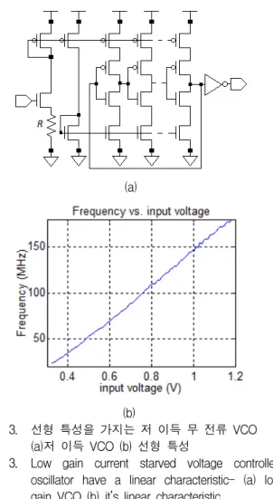
그림 3. 선형 특성을 가지는 저 이득 무 전류 VCO (a)저 이득 VCO (b) 선형 특성
Fig. 3. Low gain current starved voltage controlled oscillator have a linear characteristic- (a) low gain VCO (b) it’s linear characteristic.
VCO, are affected by supply voltage variations as well as ground noise. This problem is solved by a charge pump[5]. The output of the PFD contains the desired dc component and undesired high frequency components.
Therefore, to obtain the dc component, a RC low pass passive filter is used as a loop-filter. For the slow change in Δϕ, the loop filter acts as an integrator to find the average output of a PFD. On the other hand, for a fast change, it tracks the time differences of the rising edges or acts as a voltage divider[5].
A low gain voltage controlled oscillator produces a high frequency signal at the output in proportion to the input voltage, and will have linear characteristics for having low gain[5] as shown in Figure 3. The frequency of the oscillation of the VCO can be given by the (1) for the Id drain current of n stages of the CS inverter[5, 12].
(1)
where
(2)
C
ox can be determined by εox/Tox, where εox is the electrical permittivity and Tox is the thickness of the SiO2 layer of a MOS, and assuming channel widthW = W
p/2 = W
nand channel length
L = L
p =L
n.One of the important quality factors for determining the performance of a PLL is the variation in the period of the output signal in the time domain, which is known as jitter[5, 13]. For the Δ
f
VCO frequency deviation of the VCO output, jitter, Δt
jit, can be estimated using (3)[5].∆
∆
(3)
The duty cycle of a
VCO
out must be 50% to avoidjitter and instability.
Ⅲ. Proposed Phase Frequency Detector
Sometimes the up (or dn) needs to be Hi to increase (or decrease) the frequency of the dclk.
Because a PFD consists of edge triggered two D flip-flops and, data and dclk are connected to the clock of the flip-flops, it will change the output when there is a positive going transition (PGT) in data (or
dclk). Therefore, if it is not changing immediately
when required, a PGT can be inserted by a simple combinational circuit, as shown in Figure 4, when it is needed before the actual transition. Because the combinational circuit or pre-coder uses only inverters and a XOR gate, the output of it will preserve the phase and frequency information of the data signal.Inverted Delay
Unit
XORGate
data to
PFD
(a)
(b)
그림 4. 전-부호기 (a) 블록도, (b) 제안한 PFD의 전-부 호기의 입력 및 출력 파형 형태
Fig. 4. Pre-coder (a) block diagram, and (b) Input and output wave forms of the pre-coder of the proposed PFD.
그림 5. 제안한 DPLL의 블록도
Fig. 5. Block diagram of the proposed DPLL.
An odd number of inverters were used to obtain the delayed and inverted version of the data signal, and a XOR gate[6] was used in pre-coder to combine the original data with a delayed and inverted signal of the data. In this way, a PGT can be inserted in the marked position, as shown in Figure 4(b) and Figure 5 shows the proposed architecture with the new PFD.
Ⅳ. Design and Simulation Results
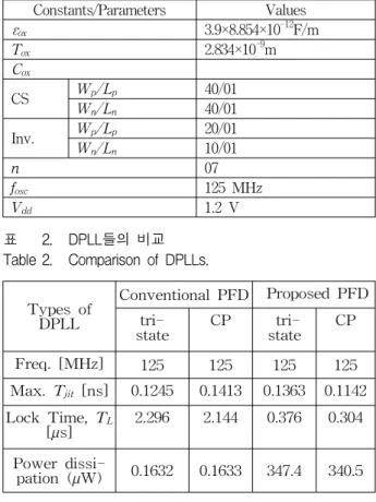
The maximum frequency deviation estimated fromConstants/Parameters Values
ε
ox 3.9×8.854×10-12F/mTox 2.834×10⁻⁹m
Cox
CS Wp/Lp 40/01
Wn/Ln 40/01
Inv. Wp/Lp 20/01
Wn/Ln 10/01
n 07
fosc 125 MHz
Vdd 1.2 V
표 1. 상수들과 설계 파라미터들
Table 1. Constants and Design Parameters.
Types of DPLL
Conventional PFD Proposed PFD tri-
state CP tri-
state CP
Freq. [MHz] 125 125 125 125
Max. Tjit [ns] 0.1245 0.1413 0.1363 0.1142 Lock Time, TL
[µs] 2.296 2.144 0.376 0.304 Power dissi-
pation (µW) 0.1632 0.1633 347.4 340.5
표 2. DPLL들의 비교
Table 2. Comparison of DPLLs.
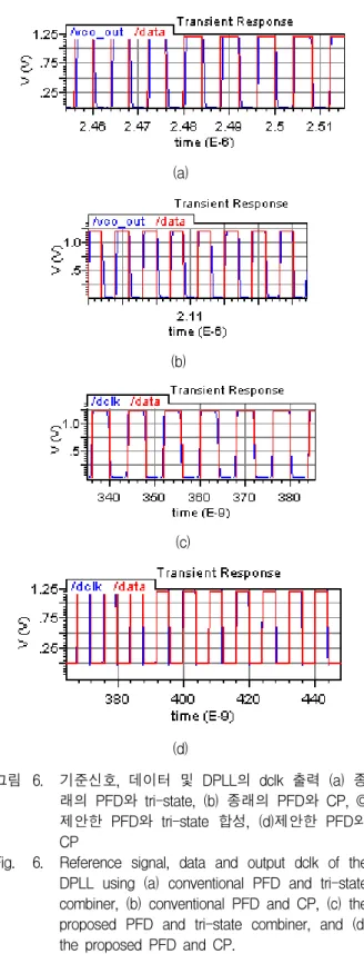
(a)
(b)
(c)
(d)
그림 6. 기준신호, 데이터 및 DPLL의 dclk 출력 (a) 종 래의 PFD와 tri-state, (b) 종래의 PFD와 CP, © 제안한 PFD와 tri-state 합성, (d)제안한 PFD와 CP
Fig. 6. Reference signal, data and output dclk of the DPLL using (a) conventional PFD and tri-state combiner, (b) conventional PFD and CP, (c) the proposed PFD and tri-state combiner, and (d) the proposed PFD and CP.
the simulation result and hence the jitters, mentioned in Table 2, are the maximum values, not the conventional rms or average values. The design parameters, as mentioned in Table 1, were calculated according to the specifications and then circuit sizing
was performed using the design parameters to satisfy the specifications. Afterwards, the DPLL was simulated and different design parameters were optimized until the desired output was found. In here, four DPLLs were designed, which are as follows: (a) DPLL with conventional PFD and tri-state combiner, (b) DPLL with conventional PFD and CP, (c) DPLL with the proposed PFD and tri-state combiner and (d) DPLL with the proposed PFD and CP. When the output signal dclk of the DPLL is locked with the input reference signal data, the edges of dlck align with that of data, which has been shown in Figure 6 for above mentioned four cases.
From the simulation it was found that the conventional PFD and tri-state combiner based DPLL took 2.296 µs to lock with a maximum jitter of 0.1245 ns. Similarly, the DPLL with a conventional PFD and CP took 2.144 µs to lock with a maximum jitter of 0.1413 ns. On the other hand, the DPLLs with a tri-state or CP combiner with the proposed PFD took 0.376 µs and 0.304 µs, respectively, to lock, and the CP based proposed DPLL has a jitter of only 0.1142 ns.
V. Conclusions
The above mentioned design method was used extensively to design the PFD, inverted phase detectors, loop filter, and 7-stage CS VCO. The W/L and others parameters in Table 1 are the optimized values. The results showed that the conventional PFD-based DPLL with a tri-state combiner took a long time, 2.296 µs, to lock with a maximum jitter of 0.1245 ns, which is less than 2.5% of its period 8 ns [5]. On the other hand, the DPLL with a conventional PFD and CP took 2.144 µs to lock with a higher
jitter than the previous one but the value was still
lower than the rule of thumb- 2.5% of its period.The performance of the DPLL was improved significantly by the addition of a PGT when required before the actual time using the proposed PFD.
DPLLs with the proposed PFD and a tri-state or CP, took less time i.e. 0.376 µs and 0.304 µs, respectively, to lock, and the CP based proposed DPLL had the lowest jitter of only 0.1142 ns. Therefore, using the proposed architecture or inserting a PGT in the data (or dclk) signal to change the output, up or dn to minimize the lock time and jitter significantly.
REFERENCES
[1] Kim H.S., et. al. “A Digital Fractional-N PLL With a PVT and Mismatch Insensitive TDC Utilizing Equivalent Time Sampling Technique,”
IEEE Journal of Solid-State Circuits, Vol. 48, No. 7, 2013.
[2] Nagaraj, K., et. al. “Architectures and Circuit Techniques for Multi-Purpose Digital Phase Lock Loops,” IEEE Transactions on Circuits and Systems, Vol. 60, Issue: 3, 2013.
[3] Ni Xu, Woogeun Rhee, and Zhihua Wang,
“Semi-digital PLL Design for Low-Cost Low-Power Clock Generation,” Journal of Electrical and Computer Engineering, Vol. 2011:
1-9, 2011.
[4] B. Razavi, “Design of Analog CMOS Integrated Circuits,” Los Angeles: McGraw-Hill, International Edition, 2001.
[5] R. J. Baker, “CMOS: Circuit Design, Layout and Simulation,” New Jersey: Wiley-IEEE press, 3rd Edition, 2010.
[6] Jin-Ku Kang and Dong-Hee Kim, “A CMOS Clock and Data Recovery with Two-XOR Phase-Frequency Detector Circuit,” The 2001 IEEE International Symposium on Circuits and Systems, ISCAS, 2001.
[7] H. Kondoh, H. Notani, T. Yoshimura and Y.
Matsuda, “A 1.5V 250MHz to 3.3V 622MHz CMOS phase locked loop with precharge type CMOS phase detector,” IEICE Trans. Electron, Vol.: E78-C, No. 4, pp.381-338, 1995.
[8] H. O. Johansson, “A simple Precharged CMOS Phase Frequency Detector,” IEEE Journal of Solid-State Circuits, Vol.: 33, No. 2, pp. 295-299, 1998.
[9] D. Efstathiou, “A Digital Loop Filter for a Phase Locked Loop,” 17th International Conference on Digital Signal Processing, pp.1-6, 2011.
[10] Ian A. Young, Jeffrey K. Greason, and Keng L.
Wong, “A PLL Clock Generator with 5 to 110 MHz of Lock Range for Microprocessors,” IEEE Journal of Solid-State Circuits, Vol. 27, No. II, pp.1599-1607, 1992.
[11] Y. Ji-Ren, I. Karlsson, C. Svensson, “A True Single-Phase-Clock Dynamic CMOS Circuit Technique,” IEEE Journal of Solid-State Circuits, Vol. SC-22, No. 5, 1987.
[12] D. Ghai, S. P. Mohanty and E. Kougianos,
“Design of Parasitic and Process-Variation Aware Nano-CMOS RF Circuits: A VCO Case Study,” IEEE Transactions on Very Large Scale Integration (VLSI) Systems, Vol. 17, No. 9, 2009.
[13] Roland E. Best, “Phase-Locked Loops Design, Simulation and Applications,” New York: 6th edition, McGraw-Hill, 2007.
저 자 소 개
Md. Tariq Hasan(학생회원) 2001년 Khulna University
전자통신공학과 학사졸업 2013년 현재 조선대학교
정보통신공학과 석사과정 2002년~2006년 Khulna Univ.
전자통신공학과 강사.
2006년~Khulna Univ. 전자통신공학과 조교수.
<주관심분야 : 통신 VLSI ASIC, ASIP 디자인, 채널 부호>
최 광 석(평생회원)
1987년 부산대학교 전자공학과 학사 졸업.
1989년 부산대학교 전자공학과 석사 졸업.
2002년 고려대학교 전자공학과 박사 졸업.
1989년~2006년 삼성전자 DM연구소 수석연구원 2012년 현재 조선대학교 정보통신공학과 부교수
<주관심분야 : 통신 및 디지털 미디어 SOC설 계>