A Design of LC-tuned Sinusoidal VCOs Using OTA-C Active Inductors
Won-Sup Chung
*★and Sang-Hee Son
*Abstract
Sinusoidal voltage-controlled oscillators (VCOs) based on Colpitts and Hartley oscillators are presented.
They consist of a LC parallel-tuned circuit connected in a negative-feedback loop with an OTA-R amplifier and two diode limiters, where the inductor is simulated one realized with temperature-stable linear operational transconductance amplifiers (OTAs) and a grounded capacitor. Prototype VCOs are built with discrete components. The Colpitts VCO exhibits less than 1% nonlinearity in its current-to-frequency transfer characteristic from 4.2 to 21.7 MHz and ±95 ppm/℃ temperature drift of frequency over 0 to 70℃. The total harmonic distortion (THD) is as low as 2.92% with a peak-to-peak amplitude of 0.7 V for a frequency-tuning range of 10.8-32 MHz. The Hartley VCO has the temperature drift and THD of two times higher than those of the Colpitts VCO.
Key words: Analog circuit, Voltage-controlled oscillator, Active inductor, Operational transconductance amplifier, Colpitts and Hartley oscillators
*Department of Semiconductor Engineering, Cheongju University, Cheongju 360-764, Korea.
★ Corresponding author
W.-S. Chung is with the Department of Semi- conductor Engineering, Cheongju University, Cheongju 360-764, Korea.
Manuscript received April. 30, 2007 ; revised Agust. 7, 2007
I. Introduction
Voltage (current)-controlled oscillators (VCOs) with sinusoidal outputs have a number of important applications in instrumentation, measurement, and communication systems. Sinusoidal VCOs with wide sweep capability can be realized by using operational transconductance amplifiers (OTAs) as active components [1]-[3]. In these realizations, the variation of the oscillation frequency is obtained by controlling the transconductance gain of the OTA incorporated in the frequency-determining network.
Since the transconductance gain of the OTA can be varied by an external dc bias current, the VCO operation can be readily implemented. The OTA-based VCOs reported so far are generated from four classical oscillator models, namely the
phase-shift [1], the Wien-bridge [4], the quadrature
5]-[7], and the state-variable bandpass oscillators [8]. These VCOs exhibit relatively wide frequency sweep ranges, but do not provide sufficient frequency stability to use them as a precise component in the design of instrumentation and measurement systems.
LC-tuned oscillators have higher frequency stability than RC-active oscillators mentioned above.
Therefore, VCOs with higher stability can be generated from LC-tuned oscillator models [9]; the positive-feedback LC-tuned oscillator(bandpass-filter-based oscillator) and the negative-feedback one (Colpitts and Hartley oscillator). Several circuits are available in the literature for the realization of VCOs based on the former oscillator [10]-[11]. In these VCOs the inductors are simulated by interconnecting two matched OTAs and a grounded capacitor, and the resultant equivalent inductances are inversely proportional to the square of the transconductance gain of OTAs. The simulated inductor (or active inductor) in turn together with a capacitor forms a
LC resonant (bandpass) circuit to determine the oscillation frequency. A main disadvantage of these VCOs is that they exhibit narrow sweep capability and relatively poor frequency stability with regard to temperature when the circuits oscillate at high frequency (over several MHz).
In this paper alternative LC-tuned VCOs with wide sweep capability and superior frequency stability is presented. These VCOs are based on Colpitts and Hartley oscillator operating at high frequency.
II.
Circuit Description and Operation1. Colpitts VCO
Fig. 1 shows the circuit diagram of an OTA-RC Colpitts VCO, in which four identical OTAs marked
and a grounded capacitor
form an active floating inductor. The VCO consists of a LC parallel-tuned circuit connected in a negative-feedback loop with an OTA-R amplifier and two diode limiters. Diode limiters are used to limit the input signal voltages of OTAs within their linear ranges (about ±V). Disregarding the limiter circuits and assuming ideal OTAs, routine analysis yields the loop gain of the oscillator circuit given by
(1)
where
is the transconductance of gain of OTA1.R
D3 D4 D1 D2
1
Gm
C1 C2
C Gm Gm
Gm Gm
vO
Fig. 1. Circuit diagram of an OTA-
RC
Colpitts VCO.The phase of the loop gain will be zero at one frequency given by
(2)
To obtain sustained oscillations at this frequency, the magnitude of the loop gain should be set to unity. This can be achieved by selecting
(3)From (2) and (3), it is obvious that the frequency of oscillation can be linearly controlled by adjusting the transconductance gains of the OTAs marked
without affecting the condition of oscillation.Since the transconductance gain is a function of a dc bias current, it can be seen that linear current (voltage)-to-frequency conversion is obtainable.
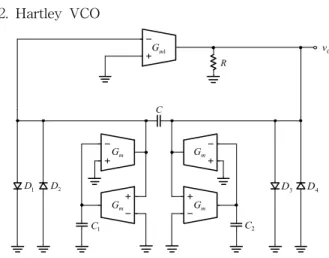
2. Hartley VCO
D3 D4
D1 D2
Gm 1
Gm
C1 C2
C
R
vO
Gm
Gm Gm
Fig. 2. Circuit diagram of an OTA-
RC
Hartley VCO.Fig. 2 shows the circuit diagram of an OTA-RC Hartley VCO, in which left two identical OTAs marked
and a grounded capacitor
form one grounded inductor and right two identical OTAs and a grounded capacitor
form the other grounded inductor. The VCO consists of a LCparallel-tuned circuit connected in a negative- feedback loop with an OTA-R amplifier and two diode limiters. Disregarding the limiter circuits and assuming ideal OTAs, routine analysis yields the loop gain of the oscillator circuit given by
(4)
From (4) one can obtain the oscillation conditions, and the results are given by
(5)
(6)From (5) and (6), it is obvious that the frequency of oscillation can be linearly controlled by adjusting the transconductance gains of the OTAs marked
without affecting the condition of oscillation.Ⅲ. Temperature-Stable Linear OTA
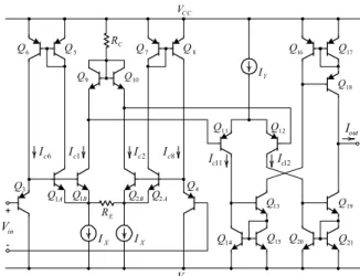
It is clear from (2) and (5) that in OTA-based oscillators the frequency stability is directly related to the temperature-dependency of OTA. Therefore, the temperature-stable OTA is essential element in the design of VCOs with high frequency stability. A circuit diagram of a temperature-stable linear OTA designed for the OTA-based LC-tuned VCO is shown in Fig. 3. It consists of a linear transconductor formed by transistors
-
and an emitter-degeneration resistor
, a translinear current gain cell
-
, and three Wilson current mirrors
-
. The transconductor converts the differential input voltage
into its corresponding differential output currents
and
[12],
(7a)
(7b)
VCC
VEE
Iout
RC
RE
IX
IX
Q1B Q2B Q2A
Q1A
Q3 Q4
Q6 Q5 Q7 Q8
Q9 Q10 IY
Q11 Q12
Q13
Q14 Q15
Q16 Q17
Q18
Q19
Q20 Q21 Vin
+
-
1
Ic Ic8
11
Ic Ic12
6
Ic Ic2
Fig. 3. Circuit diagram of a temperature-stable linear OTA designed for the VCOs.
The differential output currents
,
of the transconductor drive the diode-connected transistor pair
and
of the translinear current gain cell.The current gain cell makes the current partitioning of the transistor pair
and
to be the mirror image of the current partitioning of the transistor pair
and
[13]. Therefore, we can write the following relation:
(8)
The output currents
and
of the current gain cell are differenced by three current mirrors formed by
-
,
-
, and
-
, respectively. Since the sum of
and
is
and the difference is
, which denotes the single-ended output current of the OTA, currents
and
can be written as follows:
(9a)
(9b)
Combining (7a), (7b), (8), (9a), and (9b), one can obtain the transfer function of the OTA expressed as follows:
(10)The transconductance gain
is given by
. It should be noted that the tansconductance gain of the OTA is independent of temperature and determined by the ratio of the dc bias currents
and
. It can be shown from (7a) and (7b) that the input linear range of the OTA is
≤
(11)Ⅳ. Experimental Results
The OTA circuit shown in Fig. 3 was simulated using SPICE. The transistor arrays used for the OTA were HFA3096, while the resistors were
㏀. The current sources were implemented with a simple current-mirror circuit.The bias current
was set to 1 mA in order to obtain an input linear range of ± V. All measurements were performed at supply voltages of
V,
V. The dc transfer characteristic of the simulated circuit for a fixed
of 1 mA is plotted in Fig. 4. The linearity error is seen to be less than 1.1 % in the differential input ranges of ±V.Input voltage vIN [ V ]
-2 -1 0 1 2
Output current IOUT [ mA ]
-1.5 -1.0 -0.5 0.0 0.5 1.0 1.5
Linearity error [ % ]
-2 -1 0 1 2 Dc transfer curve
Linearity error
Fig. 4. Simulated dc transfer characteristic of the OTA.
Temperature [ oC ]
0 20 40 60
Transconductance gain Gm [ mS ]
0.0 0.2 0.4 0.6 0.8 1.0 1.2 1.4
C ppm/
5 . 88 μA,
100 o
Y= I
C ppm/
7 . 32 μA,
500 o
Y= I
C ppm/
9 . 9 mA,
1 - o
Y= I
Fig. 5. Simulated temperature characteristic of the OTA.
The dependency of the transconductance on temperature is shown in Fig. 5, which shows that the effect of temperature on thetransconductance is almost negligible (less than 90 ppm/℃). This result is 12 times better than that obtained from the previous work [12]. The open-loop bandwidth of the simulated OTA with
mA was 400 MHz.Breadboard prototype VCOs of Fig. 2 and Fig.
3 have been devised using the OTA shown in Fig.
3, 0.5-tolerance resistors, and polystyrene capacitors.
For the Colpitts VCO the relation between the frequency of oscillation and the bias current
was measured with
= 10 pF,
=
= 2 pF,
= 1 k, and
= 0.5 mA, while for the Hartley VCO the relation was measured with
= 1 pF,
=
= 8 pF,
㏀, and
= 0.5 mA,. The results are plotted in Fig. 6, which shows that the frequency of the VCOs is linearly controllable by the bias current
over the frequency range of 4.22-21.72 MHz with the linearity error less than 1%. For comparison, the relation between the frequency and the bias current obtained by the conventional bandpass-filter (BPF)-based VCO in [11] is also shown in Fig. 6. It exhibits a narrow frequency control range of 19.6-27.3 MHz.Sweep range (MHz)
Frequency stability (ppm/℃)
BP- VCO Colpitts
- VCO Hartley-
VCO [2]
[5]
[7]
19.6-25.68 0.7-40 0.4-40
0.15-0.25 3-10.3
2-11 0.02-0.55
±115
±95
±220
- - - - Bias current IY [ mA ]
102 103
Oscillation frequency f0 [ MHz ]
10-1 100 101 102
Colpitts-VCO Hartley-VCO BPF-VCO
Fig. 6. Measured frequency of oscillation against the bias current for each VCO.
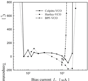
The temperature stability of the oscillator frequency was measured over a temperature range of 0 to 70℃. The results are plotted in Fig. 7, indicating that the temperature drift of the Colpitts VCO is less than ±95 ppm/℃ over the frequency range of 1.36-40.9 MHz, while the Hartley VCO has the temperature drift of about two times higher than that of the Colpitts VCO. The peak-to-peak
Bias current IY [ mA ]
102 103
Temperature stability [ ppm/o C ]
-200 0 200 400 600 800
Colpitts-VCO Hartley-VCO BPF-VCO
Fig. 7. Measured temperature stability of frequency for each VCO.
Bias current IY [ mA ]
102 103
THD [ % ]
0 5 10 15 20 25 30
Colpitts-VCO Hartley-VCO BPF-VCO
Fig. 8. Measured THD of the output sine wave for each VCO.
amplitudes of the output sine waves were measured.
The results showed that the peak-to-peak amplitudes is almost constant at 0.7 V up to 10.85 MHz and then slowly increases as the oscillation frequency increases. The total harmonic distortions (THDs) of the output sine waves for each VCO are plotted in Fig. 8, indicating that the THD of the Colpitts VCO is as low as 2.92 percent over the frequency range of 10.85-32.02 MHz, while the THD of the Hartley VCO is about two times higher than that of the Colpitts VCO. A performance comparison of other sinusoidal oscillator circuits is shown in Table 1.
Table 1. Performance Comparison other sinusoidal oscillator circuits
[8]
[11] 0.45-45(kHz) -250
Ⅴ. Conclusions
New LC-tuned sinusoidal VCOs based on Colpitts and Hartley oscillators have been d* escribed. In these VCOs inductors are implemented with temperature-stable OTAs and grounded capacitors. The VCOs feature linear controllability of their frequency by a dc bias current. An additional feature is that they exhibit excellent frequency stability and relatively constant amplitude over a tuning range. Because of these properties, the proposed VCOs are expected to find wide applications in instrumentation and measurement systems.
References
[1] Application Specific Analog Products, Databook.
Santa Clara, CA: National Semiconductor Corp., 1995.
[2] M. T. Abuelma’atti and R. H. Almaskatti,
"Digitally programmable active-C OTA based oscillator," IEEE Trans. Instrum. Meas., vol. IM-37, pp. 166-169, June 1988.
[3] M. T. Abuelma’atti and R. H. Almaskatti, "Two new integrable active-C OTA-based linear voltage (current)-controlled oscillations," Int. J. Electron., vol. 66, pp. 135-138, 1989.
[4] R. Senani and B. A. Kumar, "Linearly tunable Wien-bridge oscillator realised with operational transconductance amplifiers," Electron. Lett., vol. 25, pp. 19-21, 1989.
[5] B. Linares-Barranco, A. Rodriguez-Vazquez, E.
Sanchez-Sinencio, and J. L. Huertas, "10 MHz CMOS OTA-C voltage-controlled quadrature oscillator," Electron. Lett., vol. 25, pp.765-766, June 1989.
[6] T. Serrano-Gotarredona and B. Linares-Barranco,
"7-decade tuning range CMOS OTA-C sinusoidal VCO," Electron. Lett., vol. 34, pp. 1621-1622, Aug.
1998.
[7] K. Salimi, F. Krummenacher, C. Dehollain, and
*
M. Declercq, "Two-stage high swing fully integrated tunable quadrature sine oscillator,"
Electron. Lett., vol. 36, pp. 1338-1339, Aug. 2000.
[8] A. Rodriguez-Vazquez, B. Linares-Barranco, J.
L. Huertas, and E. Sanchez-Sinencio, "On the design of voltage-controlled sinusoidal oscillators using OTA's," IEEE Trans. Circuits Syst., vol.
CAS-37, pp. 198-211, Feb. 1990.
[9] A. B. Grebene,
Bipolar and MOS Analog Integrated Circuit Design
. New York: Wiley, 1984, ch. 11[10] A. Thanachayanont and A. Payne, "CMOS floating active inductor and its application to bandpass filter and oscillator designs," IEE Proc.-Circuits Devices Syst., vol. 147, pp. 42-48, Feb. 2000.
[11] Hoon Kim, Jae-Woo Kim, Won-Sup Chung, Ji-Mann Park, and Hee-Jun Kim, "A LC-tuned sinusoidal VCO using temperature-stable linear OTAs," Proceedings of ITC-CSCC 2003, vol. 1, pp.
601-604.
[12] W.-S. Chung and H.-W. Cha, "Bipolar linear transconductor," Electron. Lett., vol. 26, pp. 619-620, May 1990.
[13] B. Gilbert, "A new wide-band amplifier technique," IEEE J. Solid-State Circuits, vol. SC-3, pp. 353-365, Dec. 1968.
BIOGRAPHY
Chung Won-sup Chung (Nember)
1977 : BS degree in electrical communications engineering, Hanyang University.
1979 : MS degree in electrical communications engineering, Hanyang University.
1986 : PhD degree in Electronics Engineering, Shizuoka University.
1986~ : a Professor of the Department of Semiconductor Engineering, Chongju University
Son Sang-hee Son (Nember)
1983 : BS degree in Electrical Engineering, Hanyang
University.
1985 : MS degree in Electrical Engineering, Hanyang
University.
1998 : PhD degree in Electrical Engineering, Hanyang University.
1988~1990 : a full-time lecturer of the Univ. of Soonchunhyang
1991~ : a Professor of the Department of Semiconductor Engineering, Chongju University
![Fig. 4. Simulated dc transfer characteristic of the OTA. Temperature [ o C ]02040 60Transconductance gain Gm [ mS ]0.00.20.40.60.81.01.21.4Cppm/5.88μA,100oY=ICppm/7.32μA,500oY=ICppm/9.9mA,1-oY=I](https://thumb-ap.123doks.com/thumbv2/123dokinfo/4681749.502160/4.892.471.786.189.512/simulated-transfer-characteristic-temperature-transconductance-cppm-icppm-icppm.webp)