입자 크기 분포에 따른
0.01Pb(Mg 1/2 W 1/2 )O 3 -0.41Pb(Ni 1/3 Nb 2/3 )O 3 -0.35PbTiO 3 -0.23PbZrO 3
후막의 미세구조 및 압전특성
문희규·송현철·김상종·최지원·강종윤·윤석진 †
Piezoelectric properties and microstructure of
0.01Pb(Mg 1/2 W 1/2 )O 3 -0.41Pb(Ni 1/3 Nb 2/3 )O 3 -0.35PbTiO 3 -0.23PbZrO 3 thick film with particle size distribution
Hi-Gyu Moon, Hyun-Cheol Song, Sang-Jong Kim, Ji-Won Choi, Chong-Yun Kang, and Seok-Jin Yoon †
Abstract
The PZT based piezoelectric thick films prepared by screen printing method have been mainly used as a functional material for MEMS applications due to their compatibility of MEMS process. However the screen printed thick films generally reveal poor electrical and mechanical properties because of their porous microstructure. To improve microstructure we mixed attrition milled powder with ball milled powder of 0.01Pb(Mg
1/2W
1/2)O
3-0.41Pb(Ni
1/3Nb
2/3)O
3- 0.35PbTiO
3-0.23PbZrO
3+0.1 wt% Y
2O
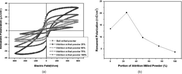
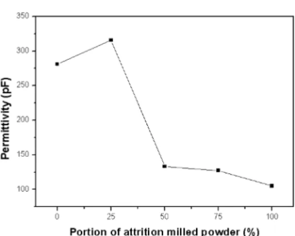
3+1.5 wt% ZnO composition. By mixing 25 % of attrition milled powder and 75 % of ball milled powder, the broadest particle size distribution was obtained, leading to a dense thick film with crack-free microstructure and improved dielectric properties. The X-ray diffraction analysis revealed that the film was in well- crystallized perovskite phase. The remanent polarization was increased from 13.7 µ C/cm
2to 23.3 µ C/cm
2at the addition of 25 % attrition milled powder.
Key Words : piezoelectric, attrition milling, thick film, MEMS
1. 서 론
압전 및 전왜 재료는 낮은 구동전압에서 큰 힘을 낼 수 있으며 , 빠른 응답특성과 간단한 시스템 구조를 가 지기 때문에 MEMS(micro electro mechanical system)
를 이용한 액츄에이터 시스템의 기능성 재료 (func- tional material) 로써 많은 연구가 진행되고 있다 . 특히
PZT 는 대표적인 압전재료로서 , 우수한 압전 특성 및
전기적 특성을 가지고 있어서 MEMS 액츄에이터에 많
이 응용되고 있으며 이에 대한 연구가 활발히 이루고 지고 있다 [1-6] .
MEMS 공정에 압전 재료를 접목하기 위해서는 압전
체를 박막 및 후막형태로 제작하여야 한다 . 압전체 박 막은 주로 PLD(pulsed laser deposition), 솔겔 (sol-
gel) [7-9] , 스퍼터링 (sputtering) 등의 방법을 이용해서 실
리콘 웨이퍼 위에 증착되어진다 . 그리고 이러한 압전체 박막은 미세한 패턴 형성이 가능하고 전기·기계적 특성 값이 우수하다는 장점을 가지고 있다 . 반면에 롤 코팅
(roll coating), 스크린 프린팅 (screen printing) [5,10,14] , 닥터 블래이드 , 가스젯 프린팅 (gas-jet) [11] 등을 이용하여 제
작되는 압전 후막의 경우 10 µ m 이상의 막을 쉽게 증 착시킬 수 있지만 , 가공성과 전기·기계적 특성 값이 박 막에 비해 떨어진다는 단점을 가지고 있다 [12] . 그리고
스퍼터링 , 솔겔 방법 등의 박막 제조 방법 또한 많은 증착 시간과 복잡한 공정 과정이 필요하며 , 일정 두께 이상으로 증착되면 내부의 스트레스의 증가로 인해 균 열이 발생하는 등 , 두께 증가에 한계를 가지고 있다 .
한국과학기술연구원
(Korea Institute of Science and Technology)
†