Fabrication and characteristics of NO x gas sensors using WO 3 and In 2 O 3 thick films to monitor air pollution
M. W. Son, J. B. Choi, H. I. Hwang * , and K. S. Yoo † Abstract
With the increasing number of automobiles, the problem of air pollution from the exhaust gases of automobiles has become a critical issue. The principal gases that cause air pollution are nitrogen oxide or NO
x(NO and NO
2), and CO.
Because NO
xgases cause acid rain and global warming and produce ozone(O
3) that leads to serious metropolitan smog from photochemical reaction, they must be detected and reduced. Mixtures of WO
3and In
2O
3(WO
3:In
2O
3=10:0, 7:3, 5:5, 3:7, and 0:10 in wt.%), which are NO
xgas-sensing materials, were prepared, and thick-film gas sensors that included a heater and a temperature sensor were fabricated. Their sensitivity to NO
xwas measured at 250~400
oC for NO
xconcentrations of 1~5 ppm. The In
2O
3thick-film sensor showed excellent sensitivity(R
gas/R
air=10.22) at 300
oC to 5-ppm NO. The response time for 70 % saturated sensitivity was about 3 seconds, and the sensors exhibited very fast reactivity to NO
x.
Key Words : air pollution, NO
xsensor, WO
3gas sensor, In
2O
3gas sensor, thick film
1. Introduction
The air pollution caused by exhaust gases of automo- biles and factories has become a critical issue. Nitrogen oxide or NO x (NO and NO 2 ) is especially toxic and causes acid rain and global warming. To prevent air pollution and eliminate NO x from the atmosphere, a sensor with high sensitivity to low-concentration NO x is needed [1-5] .
Gas sensors that use ceramics can be classified into the semiconductor type, the solid-electrolyte type, the electrochemical type, and the catalytic combustion type.
The semiconductor-type gas sensor is operated by chang- ing its conductivity when it is exposed to a specific gas [6-8] .
NO x sensing materials such as ZnO, SnO 2 , and WO 3
ceramics are still being investigated. Because they are n-type semiconductors, they have the advantages of rapid reactivity, efficiency, and gas selectivity when suitable additives are applied to them. In 2 O 3 is also an n-type semiconductor that is known as a sensing mate- rial for flammable gases such as CH 4 , C 3 H 8 , and n-
C 4 H 10 [5,9-14] .
In this study, new NO x gas sensors were fabricated using mixtures of WO 3 and In 2 O 3 (WO 3 :In 2 O 3 =10:0, 7:3, 5:5, 3:7, and 0:10 in wt.%). Their sensing property was measured using the voltage detection method. The crys- talline was confirmed via X-ray diffraction analysis.
The microstructure was observed using field emission scanning electron microscopy(FESEM).
2. Experiment
The powders of various gas-sensing materials were prepared using the solid-state reaction method, starting from the raw materials, WO 3 and In 2 O 3 . To improve the reactivity and sensitivity of the gas sensors, 0.1-wt%
PdCl 2 was added as a catalyst. The powders were mixed for 24 h using wet milling with a zirconia ball and eth- anol. The mixed powders were then dried at 50 o C for 6 h using a hot magnetic stirrer, and then calcined at 1000 o C for 4 h.
To prepare thick-film NO x gas sensors, a paste was made by mixing 10 g of the powder and 4 g of the vehi- cle(56-wt% α -terpinel, 27-wt% 2-butoxy ethoxy, 11.5- wt% polyvinyl butyral-co-vinylalcohol-co-vinyl acetate, and 16.5-wt% polyethylene glycol). Commercially avail- able alumina tiles(area: 50.8 × 50.8mm 2 , thickness: 0.4mm)
Department of Materials Science and Engineering, University of Seoul
*Convergence Components R&D Division, Korea Electronics Technology Institute
†
Corresponding author: [email protected]
(Received : June 12, 2009, Accepted : July 8, 2009)
were used as substrate materials. Each tile was laser- scribed to allow several individual sensors to be printed on the substrate. The WO 3 and In 2 O 3 layers were silk- screen-printed from the paste. The Pt electrodes were also printed with a silk screen on the designated regions before the deposition of the WO 3 and In 2 O 3 layers. The layers were dried at 60 o C for 2 h. The assemblies were sintered at 450 o C for 1 h to eliminate the vehicle, and at 900 o C for 4 h in air. A schematic diagram of the sen- sors is shown in Fig. 1. To control the operating tem- peratures, a printing paste was used to form a Pt heater at the back of the alumina substrate. Pt wires were used as lead wires and were attached using silver paste.
The gas-sensing properties were measured in a con- ventional gas-flow apparatus in the range of 1-5-ppm NO x by mixing the parent gas(500-ppm NO x in an N 2 balance) and dry synthetic air. The resistance of the sen- sor was calculated as:
(1) where R S is the resistance of the sensor, R L is the resistance of the load which was controlled to fix the output voltage to the half of the input voltage because of the change the resistance of the sensor with the change of temperature, V C is the input voltage, and V RL
is the output voltage. The resistance of the sensors was measured using a multimeter. The sensitivity, which refers to the resistance of a sensor that has been exposed to NO x gas versus the resistance of a sensor that has been exposed to air, was calculated as:
(2) where R gas is the resistance of the sensor that has been exposed to NO x gas and R air is the resistance of the sen-
sor that has been exposed to air.
The operating temperature was controlled by moni- toring the voltage and current using a power supply. The sensors were exposed to the flow of the required sample gases. In the gas mixtures of NO x /air, the NO x concen- tration varied from 1 ppm to 5 ppm. The thick films were characterized using FESEM(Hitachi, S-4300) and an X-ray diffractometer(XRD, D8 DISCOVER Bruker AXS GmbH).
3. Results and Discussion
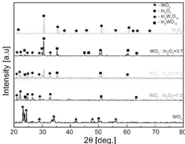
In the results of the XRD analysis that are shown in Fig. 2, the mixtures of WO 3 and In 2 O 3 are composed of the secondary phases In 2 WO 12 and In 6 WO 12 . The In 6 WO 12 phase increased but the In 2 W 3 O 3 phase dec- reased as the amount of the In 2 O 3 increased. Because secondary phases do not have a semiconductor property, the compounds that were mixed with WO 3 and In 2 O 3
were not able to detect NO x , which were consistent with the results of the sensitivity test.
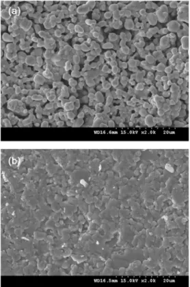
In the SEM image shown in Fig. 3, many porosities can be seen that form a reaction path between gas and oxygen on the surface. If the porosity is increased, the frequency of the adsorption-desorption of oxygen increases.
Because these sensing materials have certain degrees of porosity, they are able to detect gas [6,15] .
The sensing materials are the nonstoichiometric com- pounds. The conductivity of these n-type semiconduc- tors, such as WO 3 and In 2 O 3 , is estimated based on the electron created by the surplus metal. When sensing
R S R L V C
V RL --- 1 –
⎝ ⎠
⎛ ⎞
=
S = ( R gas ⁄ R air )
Fig. 1. Schematic view of the devices.
Fig. 2. X-ray diffraction patterns of WO
3-based powders
calcined at 1000
oC 4 h.
materials are exposed to oxidizing gases, electrons are decreased due to the reaction between the electron and the gas. Consequently, the conductivity decreases and the resistance increases
As NO x is also an oxidizing gas, electrons are decreased due to the reaction between the electrons in the sensing materials and NO x gas, as shown in the fol- lowing equations:
(3) (4) As shown in Figs. 4 and 7, when the sensors were exposed to NO x gas, their resistance increased. Because of the resistance change WO 3 and In 2 O 3 were able to detect NO x gas. Under 250 o C the resistance of the WO 3 and In 2 O 3 were very high, so they could not detect the NO x gas as there were hardly the resistance change of the WO 3 and In 2 O 3 . The highest sensitivities of the In 2 O 3
to NO x were at 300 o C, as were the highest sensitivities of the WO 3 to NO. The highest sensitivities of the WO 3
to NO 2 were at 250 o C, though.
NO 2e + – 1 2 ---N 2 + O
→
NO 2 + 2e – → NO O + 2 –
Fig. 3. SEM images of; (a) WO
3and (b) In
2O
3powders sintered at 900
oC 3 h.
Fig. 4. Gas-sensing properites of WO
3to NO.
Fig. 5. Gas-sensing properites of WO
3to NO
2.
Fig. 6. Gas-sensing properites of In
2O
3to NO.
Comparing the sensing property of In 2 O 3 with that of WO 3 , the sensitivities of In 2 O 3 to NO were higher than those of WO 3 to NO, although they were similar. The
highest sensitivity(R gas /R air ) of In 2 O 3 to 5-ppm NO was 10.22 when it was measured at 300 o C.
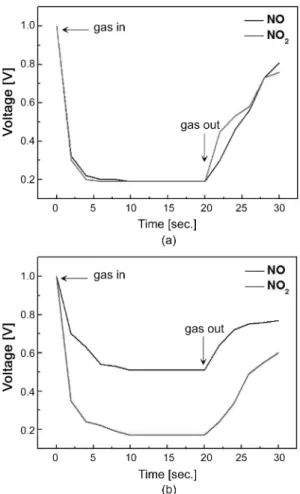
The response times of all the sensors, as shown in Fig. 8, were measured at 300 o C in 5-ppm NO x . Once the sensor was exposed to NO x , the detecting materials absorbed the gas, so the reaction between the electron and the gas was completed in 10 seconds. The response time for 70 % saturated sensitivity was especially fast at about 3 seconds. Slow recovery behavior was observed with all the sensors, though. Because perfect recovery of sensors took more than 30 sec, the voltage difference between the first and the final stage was showed in Fig. 8.
4. Summary
In this study, a sensor of NO x gas, which causes air pollution, was fabricated using mixtures of WO 3 and In 2 O 3 (WO 3 :In 2 O 3 =10:0, 7:3, 5:5, 3:7, and 0:10 in wt.%).
The crystalline of the sensing materials was confirmed via X-ray diffraction analysis. The microstructure was observed using field emission scanning electron micro- scopy(FESEM). The mixtures were not able to detect NO x because they consisted of secondary phases that had lost their semiconductor property. WO 3 and In 2 O 3 showed excellent sensing properties, though. Especially, the sensitivity of In 2 O 3 to 5 ppm NO gas at 300 o C was more than 10 and the response time for 70 % saturated sensitivity was about 3 seconds, which shows that the sensors reacted very fast to NO x gas. These results sug- gest that WO 3 and In 2 O 3 thick-films are promising sen- sor materials to monitor low-concentration NO x gas.
Acknowledgement
This work was supported by the GRRC program of Gyeonggi province. [(200811242001), Development of environmental gas-sensing materials suitable for MEMS processes]
Reference
[1] H. Kawasaki, T. Ueda, Y. Suda, and T. Ohshima,
“properties of metal doped tungsten oxide thin films for NO
xgas sensors frown by PLD method com- bined with sputtering process”, Sensors and Actua- tors B , vol. 100, pp. 266-269, 2004.
[2] U. Guth and J. Zosel, “Electrochemical solid elec-
Fig. 7. Gas-sensing properites of In
2O
3to NO
2.
Fig. 8. Respond time of (a) WO
3and (b) In
2O
3to NO
x.
trolyte gas sensors hydrocarbon and NO
xanalysis in exhaust gases”, Ionics , vol. 10, pp. 366-377, 2004.
[3] D. L. West, F.C. Montgomery, and T. R. Armstrong,
“Use of La
0.85Sr
0.15CrO
3in high-temperature NO
xsensing elements”, Sensors and Actuators B , vol.
106, pp. 758-765, 2005.
[4] Y. S. Yoon, T. S. Kim, and W. K. Choi, “Structural and electrical properties of WO
xthin films depos- ited by direct current reactive sputtering for NO
xgas sensor”, J. Kor. Ceram. Soc. , vol. 41, no. 2, pp.
97-101, 2004.
[5] K. S. Yoo, T. S. Kim, and H. J. Jung, “Fabrication and gas-sensing characteristics of NO
xsensors using WO
3thin films”, J. Kor. Ceram. Soc., vol. 32, no. 12, pp. 1369-1376, 1995.
[6] M. W. Son, J. B. Choi, H. J. Kim, S. D. Kim, and K. S. Yoo, “Fabrication and characterization of La
1-x