<연구논문>
한국표면공학회지 J. Kor. Inst. Surf. Eng.
Vol. 45, No. 6, 2012.
http://dx.doi.org/10.5695/JKISE.2012.45.6.242
High Temperature Durability Amorphous ITO:Yb Films Deposited by Magnetron Co-Sputtering
Tae Dong Jung
a, Pung Keun Song
b*a
National Core Research Center for Hybrid Materials Solution, Pusan National University, Busan 609-735, Korea
b
Department of Materials Science and Engineering, Pusan National University, Busan 609-735, Korea (Received December 29, 2012 ; revised December 29, 2012 ; accepted December 30, 2012)
Abstract
Yb-doped ITO (ITO:Yb) films were deposited on unheated non-alkali glass substrates by magnetron co- sputtering using two cathodes (DC, RF) equipped with the ITO and Yb
2O
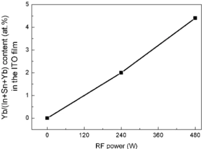
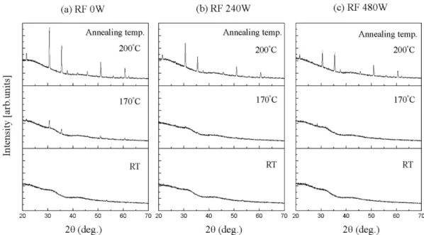
3target, respectively. The composition of the ITO:Yb films was controlled by adjusting the RF powers from 0 W to 480 W in 120 W steps with the DC power fixed at 70 W. The ITO:Yb films had a higher crystallization temperature (200ºC) than that of the ITO films (170
oC), which was attributed to both larger ionic radius of Yb
3+and higher bond enthalpy of Yb
2O
3, compared to ITO. This amorphous ITO:Yb film post-annealed at 170
oC showed a resistivity of 5.52 × 10
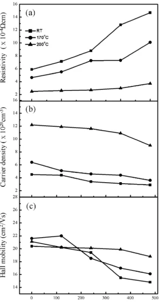
−4Ωcm, indicating that a introduction of Yb increased resistivity of the ITO film. However, these amorphous ITO:Yb films showed a high etching rate, fine pattering property, and a very smooth surface morphology above the crystallization temperature of the amorphous ITO films (about 170ºC). The transmittance of all films was >80% in the visible region.
Keywords: TCO, Yb-doped ITO, Amorphous ITO, Co-Sputtering
1. Introduction
Transparent conducting oxide (TCO) films are used widely in optoelectronic devices. In particular, indium tin oxide (ITO) films are used extensively as transparent conductive electrodes in multiple fields, such as liquid crystal displays (LCDs), plasma display panels (PDPs) and organic light emitting diodes (OLEDs) because they have high conductivity and transparency in the visible wavelength region
1-3). However, polycrystalline ITO (c-ITO) films have some disadvantages, such as rough surface morphology and low etching rate
4). Recently, with the advances in the flat panel displays (FPDs), there has been increasing demand for improvements in some of the critical properties of c- ITO films. In particular, despite the slightly higher resistivity, amorphous ITO (a-ITO) films are more attractive for FPDs applications than c-ITO films due to their excellent surface uniformity, high etching
rate, good etchability and micro-patterning
5). Some studies have examined the a-ITO deposition process through the injection of additional gas, control of the total gas pressure, or the addition of H
2O
5,6). However, these methods deteriorate the electrical properties due to the decreasing carrier density and Hall mobility.
The great part of the ITO films was produced by DC magnetron sputtering in the manufacturing line because this process has superior potential for the mass production. It is well known that film property is strongly dependent on the sintered target quality in magnetron sputtering. In addition, sintered ceramic target need to so many time to obtain high quality and optimum chemical composition in order to deposit a-ITO films without the need to control the deposition parameters. In our previous study, we confirmed that amorphous films (ITO:Ce, ITZO) showed very low surface roughness and good etchability
7-9). Therefore, in this study, we tried to prepare Yb-doped ITO (ITO:Yb) films by magnetron co-sputtering using a Yb
2O
3and ITO target because the ionic radius of
*
![Fig. 5. AFM images of the ITO and ITO:Yb films deposited with the various RF powers [RF power: (a) 0 W, (b) 240 W and (c) 480 W] at room temperature and post-annealed at different temperatures (170 o C, 200 o C)](https://thumb-ap.123doks.com/thumbv2/123dokinfo/5302487.379686/4.892.131.772.619.1136/images-deposited-various-powers-temperature-annealed-different-temperatures.webp)