• 검색 결과가 없습니다.

Hydrothermally Synthesis Nanostructure ZnO Thin Film for Photocatalysis Application

N/A
N/A
Protected

Academic year: 2021

Share "Hydrothermally Synthesis Nanostructure ZnO Thin Film for Photocatalysis Application"

Copied!
5
0
0

로드 중.... (전체 텍스트 보기)

전체 글

(1)

Manuscript received August 27, 2015, revised September 18, 2015, accepted December 1, 2015

Hydrothermally Synthesis Nanostructure ZnO Thin Film for Photocatalysis Application

수열합성법으로

합성된 산화아연 나노 구조 박막의 광촉매적 응용

N. M. Shinde, Min Sik Nam, U. M. Patil, Seong Chan Jun†

N. M. Shinde, 남민식, U. M. Patil, 전성찬†

Nano ElectroMechanical Device Laboratory, School of Mechanical Eng., Yonsei University, Seoul 120-749, Korea

[email protected]

Abstract

ZnO has nanostructured material because of unique properties suitable for various applications. Amongst all chemical and physics methods of synthesis of ZnO nanostructure, the hydrothermal method is attractive for its simplicity and environment friendly condition.

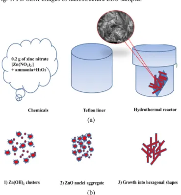
Nanostructure ZnO thin films have been successfully synthesized on fluorine doped tin oxide (FTO) substrate using hydrothermal method. A possible growth mechanism of the various nanostructures ZnO is discussed in schematics. The prepared materials were characterized by standard analytical techniques, i.e., X-ray diffraction (XRD) and Field-emission scanning electron microscopy (SEM).

The XRD study showed that the obtained ZnO nanostructure thin films are in crystalline nature with hexagonal wurtzite phase. The SEM image shows substrate surface covered with nanostructure ZnO nanrod. The UV-vis absorption spectrum of the synthesized nanostructure ZnO shows a strong excitonic absorption band at 365 nm which indicate formation nanostructure ZnO thin film.

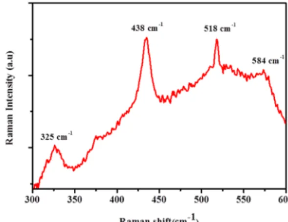
Photoluminescence spectra illustrated two emission peaks, with the first one at 424 nm due to the band edge emission of ZnO and the second broad peak centered around 500 nm possibly due to oxygen vacancies in nanostructure ZnO. The Raman measurements peaks observed at 325 cm

-1

, 418 cm

-1

, 518 cm

-1

and 584 cm

-1

indicated that nanostrusture ZnO thin film is high crystalline quality. We trust that nanostructure ZnO material can be effectively will be used as a highly active and stable phtocatalysis application.

산화아연은 다양한 나노 구조와 특유의 특성으로 인하여 여러 분야에서 많은 관심을 받고있는 물질이다. 산화아

연을 합성하는 다양한 방법 중에서, 수열합성법은 간단하고 친환경적인 장점을 가지고 있다. 나노 구조를 가지는 산 화아연 박막은 수열합성법을 통하여 FTO 전극 위에 제작되었다. 성장된 산화아연은 X-ray diffraction (XRD)와 Field- emission scanning electron microscopy (FESEM)을 통하여 분석되었다. XRD 분석에서 산화아연 박막이 자연상태의 hexagonal wurtzite 상으로 구성되어 있음을 확인하였으며 SEM 사진에서는 나노 로드 형태를 구성하고 있는 것을 확 인할 수 있었다. 본 연구에서는 UV 영역의 흡수 스펙트럼을 분석하여 산화아연이 보이는 365 nm 파장에서의 흡수를 확인하였다 . 또한 photoluminescence 방출을 분석한 결과, 424 nm의 band edge emission과 500 nm에서 산화아연의 oxygen vacancies에 의한 방출을 확인하였다. 또한 라만 스펙트럼 분석을 통하여 본 연구진이 제작한 산화아연이 높은 결정

성을 가지고 있는 것을 확인할 수 있었다. 이러한 연구를 통하여 다양한 특성을 가진 산화아연의 광촉매적 적용을

기대할 수 있다.

Keywords: Nanostructure, ZnO, thin film, hydrothermal method

I. INTRODUCTION

Creation and control nanocrystalline morphology of inorganic crystals is in materials science fields. Various nanostructures controllable morphologies have attracted wide attention because of their innovative interior design physiochemical properties. These nanomaterial properties and can lead to many potential uses. Therefore, morphology tuning with a different monocrystalline morphology property association will greatly to materials science and nanotechnology.

In the meantime, solar energy is an abundant, inexpensive and endlessly renewable source of clean energy. Converting solar energy into an easily useful form has attracted significant interest in the last several decades. Among all expertise for solar energy

conversion, photoelectrolysis has been effectively used to split water molecule into hydrogen and oxygen with no emission of toxic products. To develop superior photo catalysis electrodes and more capable devices, one of the main approaches is nanostructuring that exploits laws and specific effects at the nanoscale to enhance the efficiency of existing semiconductors and metal oxides [1]. This has grown significant attention in the last twenty years. Among current semiconductors or metal oxides, zinc oxide (ZnO) has been one of the most progressive materials.

It has been generally used in various field such as electronics,

sensors, catalysts and more energy storage devices due to its their

outstanding properties stability, environmental friendliness and

low cost. Therefore, morphology tuneable synthesis of ZnO

nanostructures is play critical role for exploring their further

(2)

potential application and scientists with great power to manipulate nanocrystaline material and device result [2]. The unique properties of nanostructured materials have wonderful motivation to explore the potentials for industrial and medical applications. The Zinc oxide is a semiconductor material with a wide band gap of 3.3 eV, which has been very useful in many applications namely optoelectronic devices, surface acoustic wave devices, field emitters, piezoelectric devices, transparent conducting materials and solar cells etc. The ZnO nanostructures are one of the most promising materials for the chemical and biosensors due to having exotic and versatile properties counting biocompatibility, nontoxicity, photochemical stability, high specific surface area, optical transparency, electrochemical activities, high electron communicating [3]-[5]. On the other hand, ZnO is form a different nanostructures morphology such as nanowires, nanoribbons/nanobelts, nanocastle, nanospheres, nanocages, nanofibers etc [6]-[8]. The above mentioned various types of nanostructures have been synthesized and extensive works have been dedicated to the development of more nanoscale structures. In which mesoporous structures of ZnO have much research interest owing to its photocatalytic applications, as they can provide more surface active sites and make easily charge carrier transport, result in to performance enhancement in all field of applications as mentioned above [9]. The absence of a centre of symmetry in ZnO wurtzite structure, with large electromechanical coupling, results in to strong piezoelectric and pyroelectric properties. In addition, ZnO is a wide band-gap (3.37eV) semiconductor hence it is suitable for short wavelength optoelectronic applications. Therefore, ZnO has been widely investigated for photo electrochemical water splitting in photoelectrolysis. Recently efficiency of ZnO in photoelectro- chemical hydrogen production is still low as a result of its relatively not more light harvesting capability and quick recombination of photo-created carriers [10]. But the ZnO shows low efficiency because its thermodynamical unstable in electrolyte solution and photo degradation. Hence, it is highly important issues to enhance the photoactivity and stability of ZnO.

To date, various semiconductors, including TiO

2

, ZnO, CdS, SrTiO

3

etc, have been applied for photocatalytic production of hydrogen [11]-[14]. ZnO has different kinetic parameters for different crystal planes, which are under controlled growth with help of experimental conditions. Thus, after an initial time of nucleation, incubation and finally crystallite growth will commonly develop into a three-dimensional with well-defined crystallographic faces [19][20]. The ZnO have encouraged research to its photocatalytic [17].

The purpose of this paper is to demonstrate a systematic study of hydrothermally synthesis nanostructure ZnO thin film for photo catalysis application. Hydrothermal method is an important method of solution synthesis because it has been proven to be synthesis of nanostructure ZnO thin film. The hydrothermal growing ZnO nanostructures has gained immense reputation due to its easy way and supportable growth conditions.

As hydrothermal synthesis is carried out in aqueous solution, hence the growth temperatures are less than the boiling point of water. The hydrothermal method could be used for the formation of nanostructures or nanostructured films almost on all substrates surface.

II. RESULTS AND DISCUSSIONS

Hydrothermal synthesis of ZnO nanrods he synthesis of ZnO was prepared by a one-step hydrothermal method. Firstly, 0.2 g of zinc nitrate [Zn(NO

3

)

2

] was added to double distilled water under constant stirring at room temperature for 5 min. Meanwhile, 25 wt% NH

3

. H

2

O was dropped slowly into the mixed solution until pH 9.0-10.0 and finally added few drop of H

2

O

2

. The mixture was then stirred continuously for 30 min. After that, 30 mL of above mixture was transferred into a Teflon-lined stainless steel reactor in which the FTO substrates were placed vertically.

The sealed autoclave was then placed in an oven at 200°C for 10 hours, after which substrates were removed and rinsed with deionized water then dried at room temperature. For the deposition of vertically aligned ZnO nanorods, the mechanism of ZnO film formation can be clarified as follows [21][22]: zinc nitrate was used as a source of Zn

2+

ions. When liquid ammonia was added into zinc nitrate solution as mentioned above, white precipitate of Zn(OH)

2

was happened, furthermore again addition of ammonia caused in to dissolution of Zn(OH)

2

in to the solution and formation of zincate ([Zn(NH

3

)

4

]

2+

). After heating, the thermal decomposition of [Zn(NH

3

)

4

]

2+

releases ions of Zn

2+

ions react with OH

in the solution and results in the formation of Zn(OH)

2

or ZnO nanorodes. All this consequence illustrates the chemical reaction as

Zn(NO

3

)

2

+ 2NH

4

OH → Zn(OH)

2

+ 2NH

4

NO

3

(1) Zn(OH)

2

+ 4NH

4

OH → [Zn(NH

3

)

4

]

2+

+ 4H

2

O + 2OH

(2) The few drop of H

2

O

2

added in the bath solution converts [Zn(NH3)4]

2+

into ZnO with the release of oxygen gas in the bath solution at higher temperature. This can be offered by the following reaction:

[Zn(NH

3

)

4

]

2+

+ 2OH− + H

2

O

2

ZnO ↓ + H

2

O + 4NH

3

↑ + 1/2O

2

↑ (3) The evolution of oxygen gas was practically detected in the form of bubbles during the deposition. The ZnO electrode materials were structurally characterized by X-ray diffraction (XRD), field-emission scanning electron microscopy (FESEM), UV-vis optical absorption, Raman spectroscopy and Photoluminescence spectra (PL) techniques. Fig. 1(a),(b) shows FE-SEM images of nanostructure ZnO samples which clearly exhibit the formation of nano rods. The well aligned vertically ZnO nanorods array on FTO substrate. Defined vertically aligned nanorods have average diameter 150 nm and length of several hundred nanometers. Such vertically aligned ZnO nanorods useful for photo catalysis application process [23][24].

As mentioned above in Fig 1(a),(b), various morphologies

of hierarchical ZnO nanostructures have been successfully

synthesized based on hydrothermal synthesis processes. These

results indicate that surfactant plays an important role in the final

morphologies of the as-prepared products. We think the growth

process of various hierarchical ZnO nanostructures can be

divided into two stages: the nucleation and the self-assembly

stages. The former is closely related to the reaction solvents,

while the after it mainly depends on the surface-active agents. A

certain amount of [Zn(NH

3

)

4

]

2+

ions dissolved in aqueous

solution has been used in for hydrothermal synthesis of hexagonal

ZnO nanostructures. Fig. 2(a),(b) shows schematic diagrams of

the experimental and growth process of nanostructure ZnO thin

(3)

film by the hydrothermal method. In growth process as shown in Fig. 2(b) included distinct steps is as 1) cluster 2) nuclei aggregation and finally formation ZnO nanostructure hexagonal rods. In the diluted ammonia aqueous solution, [Zn(NH

3

)

4

]

2+

and Zn(OH)

2

can coexist with few drops of H

2

O

2

, the amount of OH

is few (the pH value is about 10) and the formation of ZnO nuclei largely follows the reaction steps (1)→(2)→(3). In this case, the forming of ZnO nuclei is slow and it becomes the controlling step for synthesis of the nanostructure ZnO nanorods thin films.

Fig. 3 shows the XRD pattern of nanostructure ZnO thin film synthesis by hydrothermal method. The diffraction peaks in the pattern are indexed to hkl planes as (100), (002), (101), (102), (110), (103), (200), (004) and (202) respectively, which confirm the formation of nanostructure ZnO having hexagonal wurtzite phase structured. The peak assigned to the (101) plane of wurtzite diffraction peaks, the (101) plane is strongly oriented perpendicularly to the substrate surface [25]. The nanostructure ZnO sample showed a single phase nature with a hexagonal wurtzite structure.

No characteristic peaks of any other impurities are detected, which demonstrates that all of the samples have high phase purity.

The sharpness of the XRD peaks indicates the high crystallinity of the as-prepared ZnO. The intensity and FWHM of the diffraction peak was found to increase indicates that the crystalline nature of

prepared ZnO nanostructures thin film.

The average grain size was estimated according to full width with half maxima (FWHM) of diffraction peaks using Scherrer’s formula,

D 0.9

(4)

where, β is the broadening of diffraction line measured at half maximum intensity (radians) and λ = 2.2897 Å is the wavelength of the Cr Kα X-ray. The crystallite sizes of these nanostructures estimated from X-ray line broadening of (101) peak using Scherrer's equation were observed 32 nm [26]-[30].

The UV-vis optical absorption spectrum of nanostructure ZnO thin films in the wavelength range 400-850 nm has been investigated (Fig. 4). These spectra revealed that as deposited nanostructure ZnO thin films film have high absorbance of light in the visible region, indicating as an absorbing material. The absorption coefficient is higher than 10

4

cm

-1

in the visible region hence ZnO thin film is considered to be a suitable material for photovoltaic solar energy conversion. The UV-vis absorption spectrum of the synthesized nanostructure ZnO nanorod obtained a strong excitonic absorption band at 365 nm which indicate formation nanostructure ZnO thin film [31][32].

Raman spectroscopy is an active technique for confirming the crystallinity of materials. Raman scattering can give evidence about the crystal structure on the scale of a few lattice constants.

Fig. 1. FE-SEM images of nanostructure ZnO samples

(a)

(b)

Fig. 2. (a) Schematic diagrams of the experimental process of nanostructure ZnO nanorods, (b) Growth process for the formation of nanostructure ZnO thin film

Fig.3. XRD pattern of nanostructure ZnO thin film.

Fig.4. UV-vis absorption spectrum of nanostructure ZnO thin film

(4)

Therefore, Raman spectroscopic technique is one of the useful methods to achievement deep into the nanostructure structural [33]. The sharp peak at 438 cm

-1

corresponding to E

2

(low) and E

2

(high) are characteristic of hexagonal wurtzite structure of high crystalline quality (Fig.5). Peaks at 325 cm

-1

, assigned to the E2H–E2L (multiphonon process) mode for samples. Raman spectra of the nanostructure ZnO nanorod films show a broad band (BB) centered at about 518 cm

-1

[38]. The broad asymmetric peak observed at 584 cm

-1

is assigned to the 1LO mode, in agreement with reported values for bulk, thin-film and nanocrystalline ZnO [34]-[36].

The room temperature PL spectra of nanostructure ZnO thin film was obtained with an excitation wavelength of 410 nm and is shown in Fig. 6. The sharp and intense ultra violet emission peak at 424 nm is attributed to the band gap excitation, and the broad emission peak centered at 500 nm was due to oxygen vacancies in ZnO lattice [37]. In addition, the presence of a broad green emission band centered at 500 nm that lies in the visible region which is probably related to the variation of intrinsic defects in ZnO such as zinc vacancy, oxygen vacancy, interstitial zinc, interstitial oxygen and anti-site oxygen [38][39].

III. CONCLUSION

In summary, Hydrothermal synthesis of ZnO nanostructures is simple and efficient aqueous method. It was shown that films obtained nanostructure ZnO thin film by hydrothermal. This

result allows the use of hydrothermal method in its place of other chemical methods for the great excellence nanostructured ZnO thin films. The hydrothermal method was comfort for handling and the morphology of the obtained structures depended from such procedure parameter as temperature. The current results show that structures could significantly increase an active area of photo catalysts devises. The XRD, FE-SEM optical absorbance PL and Raman measurements showed that synthesis ZnO nanostructures are hexagonal phase structure. The prepared nanostructure ZnO thin films will be potential applications in the field of photo catalysis. The future study scope of ZnO nanostructures are attractive candidates for applications in field of solar cells, sensors, detectors, energy generators as well as reproduction structures for tissue engineering etc.

ACKNOWLEDGEMENT

This work was partially supported by a grant from R&D Program of the Korea Railroad Research Institute, the Yonsei University Future-leading Research Initiative of 2014 (2014-22- 0168), the Pioneer Research Center Program (2010-0019313), the Priority Research Centers Program through the National Research Foundation of Korea (NRF) funded by the Ministry of Education, Science and Technology (2009-0093823), Basic Science Research Program through the National Research Foundation of Korea (NRF) grant funded by the Ministry of Education, Science and Technology (MEST) (2013-8-0874) and Korea Electric Power Corporation though Korea Electrical Engineering & Science Research Institute (R14XA02-2).

REFERENCES

[1] X. Fan, M. L. Zhang, I. Shafiq, W. J. Zhang, C. S. Lee and S. T.

Lee,Adv. Mater., 21, 2009, 2393.

[2] M. H. Huang, Y. Wu, H. Feick, N. Tran, E. Weber and P. Yang, Adv. Mater., 13, 2001,113.

[3] Mashkoor Ahmad and Jing Zhu, J. Mater. Chem., 2011, 21, 599.

[4] Emanetoglu N W, Gorla C, Liu Y, Liang S and Lu Y 1999 Mater.

Sci. Semicond. Process 2 247.

[5] Chen Y, Bagnall D and Yao T 2000 Mater. Sci. Eng. B 75 190.

[6] Liang S, Sheng H, Liu Y, Hio Z, Lu Y and Chen H 2001, J. Cryst.

Growth 225 110.

[7] Saito N, Haneda H, Sekiguchi T, Ohashi N, Sakaguchi I and Koumoto K 2002 Adv. Mater. 14 418.

[8] Lee J Y, Choi Y S, Kim J H, Park M O and Im S 2002 Thin,Solid Films 403 533.

[9] Mitra A, Chatterjee A P and Maiti H S 1998 Mater. Lett. 35 33.

[10] Koch M H, Timbrell P Y and Lamb R N 1995 Semicond.

Sci.Technol. 10 1523.

[11] Gratzel M 2005 MRS Bull. 30 39374.

[12] Baxter J B, Walker A M, van Ommering K and Aydil E S 2006, Nanotechnology 17 S304.

[13] Lin Y, Zhang Z, Tang Z, Yuan F and Li J 1999 Adv. Mater. Opt.

Electron. 9 205.

[14] Padmavathy N and Vijayaraghavan R 2008 Sci. Technol. Adv.

Mater. 9 035004.

[15] Iijima S 1991 Nature 354 56.

[16] Cui Y, Lauhon L J and Gudiksen M S 2001 Appl. Phys. Lett.78 2214.

[17] Burghard G M, Kim G T, Dusberg G S, Chiu P W, Krstic V,Roth S and Han W Q 2001 J. Appl. Phys. 90 5747.

[18] Duan X, Huang Y, Cui Y, Wang J and Lieber C M 2001 Nature.

Fig.5. Raman spectrum of nanostructure ZnO thin film

Fig. 6. PL spectrum of nanostructure ZnO thin film

(5)

409 66.

[19] Bai Z G, Yu D P, Zhang H Z, Ding Y, Gai S Q, Hang X Z, Hiong Q L and Feng G C 1999 Chem. Phys. Lett. 303 311.

[20] Huang M H, Wu Y, Feick H, Tran N, Webe E and Yang P 2001, Adv. Mater. 13 113.

[21] Huang M H, Mao S, Feick H, Yan H, Wu Y, Kind H, Weber E,Russo R and Yang P 2001 Science 292 1897.

[22] Shi G, Mo C M, Cai W L and Zhang L D 2005 Solid State Commun.

115 253.

[23] Baruah S, Thanachayanont C and Dutta J 2008 Sci. Technol.Adv.

Mater. 9 025009.

[24] K.V. Gurav, U. M. Patil, S.W. Shin, S. M. Pawar, J. H. Kim, C. D.

Lokhande, J. Alloys Compd. 525, 2012, 1.

[25] Hu Wang, Juan Xie, Kangping Yan, and Ming Duan, J. Mater. Sci.

Technol., 2011, 27(2), 153.

[26] Ashwini P. Bhirud, Shivaram D. Sathaye, Rupali P. Waichal, Latesh K. Nikam and Bharat B. Kale, Green Chem., 2012, 14, 2790.

[27] Xiaolong Ren,Pengzhan Ying,Zuobao Yang,Minghui Shang,Huilin Hou and Fengmei Gao. RSC Adv.,2015, 5, 16361.

[28] Faheem Ahmed, Nishat Arshi, M. S. Anwar, Rehan Danish and Bon Heun Koo, RSC Adv., 2014,4, 29249.

[29] Q. Kuang, Z. Y. Jiang, Z. X. Xie, S. C. Lin, Z. W. Lin, S. Y. Xie, R. B. Huang and L. S. Zheng, J. Am. Chem. Soc., 2005, 127, 11777–11784.

[30] S. Cho, S. H. Jung and K. H. Lee, J. Phys. Chem. C, 2008, 112, 12769–12776.

[31] J. Shi, H. Hong, Y. Ding, Y. A. Yang, F. Wang, W. B. Cai and X. D. Wang, J. Mater. Chem., 2011, 21, 9000–9008.

[32] W. W. Lee, J. Yi, S. B. Kim, Y. H. Kim, H. G. Park and W. I. Park, Cryst. Growth Des., 2011, 11, 4927–4932.

[33] C. W. Cheng, B. Liu, H. Y. Yang, W. W. Zhou, L. Sun, R. Chen, S.

F. Yu, J. X. Zhang, H. Gong, H. D. Sun and H. J. Fan, ACS Nano, 2009, 3, 3069–3076.

[34] Du, L. R. Espelt, I. A. Guzei and T. P. Yoon, Chem. Sci., 2011, 2, 2115 RSC.

[35] Q. J. Xiang, J. G. Yu and M. Jaroniec, Chem. Soc. Rev., 2012, 41, 782 RSC.

[36] K. F. Zhou, Y. H. Zhu, X. L. Yang, X. Jiang and C. Z. Li, New J.

Chem., 2011, 35, 353 RSC.

[37] J. T. Zhang, Z. G. Xiong and X. S. Zhao, J. Mater. Chem., 2011, 21, 3634.

[38] Q. Shen, W. Zhang, Z. P. Hao and L. D. Zou, Chem. Eng. J., 2010, 165, 30.

[39] F. Y. Shen, W. X. Que, Y. L. Liao and X. T. Yin, Ind. Eng. Chem.

Res., 2011, 50, 9131.

[40] Jamuna K. Vaishnav, Sudhir S. Arbuj, Sunit B. Rane and Dinesh P.

Amalnerkar, RSC Adv.,2014,4,47637-47642.

[41] T.C. Damen, S.P.S. Porto, B. Tell, Phys. Rev. 142 (1966) 570.

[42] A. Sayari, A. Marzouki, A. Lusson, M. Oueslati, V. Sallet, Thin Solid Films, 2010,518, 6870–6875.

[43] B. Yang, A. Kumar, P. Feng, R.S. Katiyar, Appl. Phys. Lett. 92

(2008) 233112.

수치

Fig. 2. (a) Schematic diagrams of the experimental process of nanostructure ZnO nanorods, (b) Growth process for the formation of nanostructure ZnO thin film
Fig. 6. PL spectrum of nanostructure ZnO thin film

참조

관련 문서

The ultraviolet-visible (UV-vis) absorbance spectra of the SBDDVE films obtained from sCVD showed identical optical band edge over the film thickness range of 100 nm to 1.8