Voltage Scaling 기반의 저전력 전류메모리 회로 설계
여성대*․김종운*․조태일*․조승일**․김성권***
Design of Low Power Current Memory Circuit based on Voltage Scaling
Sung-Dae Yeo*․Jong-Un Kim*․Tae-Il Cho*․Seung-Il Cho*․Seong-Kweon Kim**
요 약
무선통신시스템은 한정된 에너지를 갖는 배터리를 사용하기 때문에 저전력 회로로 구현되어야 하며, 이를 위 하여 주파수와 상관없이 일정한 전력을 나타내는 전류모드 회로가 연구되어왔다. 본 논문에서는 초저전력 동작 이 가능하도록 Dynamic Voltage Scaling 전원을 유도하며, 전류모드 신호처리 중 메모리 동작에서 저장된 에너 지가 누설되는 Clock-Feedthrough 문제를 최소화하는 전류메모리 회로를 제안한다. 0.35µm 공정의 BSIM3 모델 로 Near-threshold 영역의 전원 전압을 사용한 시뮬레이션을 진행한 결과, 1MHz의 스위칭 동작에서 2µm의 메 모리 MOS Width, 0.3µm의 스위치 MOS Width, 13µm의 Dummy MOS Width로 설계할 때, Clock-Feedthrough 의 영향을 최소화시킬 수 있었으며 1.2V의 Near-threshold 전원전압에서 소비전력은 3.7µW가 계산되었다.
ABSTRACT
A wireless communication system is required to be implemented with the low power circuits because it uses a battery having a limited energy. Therefore, the current mode circuit has been studied because it consumes constant power regardless of the frequency change. However, the clock-feedthrough problem is happened by leak of stored energy in memory operation. In this paper, we suggest the current memory circuit to minimize the clock-feedthrough problem and introduce a technique for ultra low power operation by inducing dynamic voltage scaling. The current memory circuit was designed with BSIM3 model of 0.35µm process and was operated in the near-threshold region. From the simulation result, the clock-feedthrough could be minimized when designing the memory MOS Width of 2µm, the switch MOS Width of 0.3µm and dummy MOS Width of 13µm in 1MHz switching operation. The power consumption was calculated with 3.7µW at the supply voltage of 1.2 V, near-threshold voltage.
키워드
Current Mode Signal Processing, Current Memory, Clock-Feedthrough, DVS, Near-Threshold 전류 모드 신호 처리, 전류 메모리, 클록 피드 스루, DVS, 근접 임계
* 서울과학기술대학교 NID융합기술대학원([email protected], [email protected], [email protected])
ㆍReceived : Dec. 24, 2015, Revised : Feb. 13, 2016, Accepted : Feb. 24, 2016 ㆍCorresponding Author : Seong-Kweon Kim
Ⅰ. 서 론 유비쿼터스 센서 네트워크 (USN : Ubiquitous Sensor Network)의 실현을 위해 음성, 사진, 동영상 http://dx.doi.org/10.13067/JKIECS.2016.11.2.159
등의 멀티미디어 통신의 수요가 급증하고 있으며 이에 따라, 다양한 통신 방식의 적용연구 등이 활발히 진행 되어오고 있다[1-3]. 무선통신시스템은 한정된 에너지 의 배터리를 사용하기 때문에 통신의 지속성과 이동성 을 확보하는 것이 매우 제한적이다. 따라서 통신 시스 템이 저전력으로 동작해야하며 이를 위하여 저전력 동 작의 무선통신용 LSI(: Large Scale Integrated circuit)의 연구 및 개발이 반드시 필요하다[4-5].
특히 멀티미디어 통신을 위하여 고속 동작의 신호 처리가 요구된다. Digital 전압모드 신호처리는 동작 주파수에 비례하여 소비전력이 선형적으로 증가하여, 소비전력 절감에 매우 불리하다. 따라서 동작 주파수 에 관계없이 일정한 소비전력을 유지하는 전류모드 신호처리에 주목하여 연구를 진행하여 왔다[6]. 전류 모드 신호처리는 스위칭의 동작으로 다양한 소비전력 절감 기법이 적용될 수 있으며 바이어스 전류 동작으 로 신호처리를 수행하기 때문에 동작주파수와 무관하 게 전력을 소비함으로써 소비전력 절감 측면에서 매 우 우수한 특징을 가지고 있다. 또한 전류모드 신호처 리는 전류 Mirror 회로를 기본적으로 사용하기 때문 에 Summation, Inverting, Scaling, Memory 동작 등 디지털 신호처리의 연산 동작이 가능하다. 메모리 동 작을 담당하는 전류메모리 회로는 MOS(: Metal Oxide Semiconductor)로 설계된다. 하지만 MOS 트 랜지스터의 기생 커패시터에 저장되는 전하량으로 입 력전류를 저장하는 동작에서 스위칭 동작에 의해서 Clock-Feedthrough 현상이 발생되어 전류메모리의 성능을 저하시키는 문제점이 발생한다[7-9].
따라서 본 논문에서는 1MHz의 기저대역 (Baseband)에서 동작하며 Clock-Feedthrough 문제를 최소화하는 전류메모리 회로를 설계한다. 또한, 소비 전력 절감을 위하여 트랜지스터를 Near-threshold 영 역에서 동작시키는 Dynamic Voltage Scaling 회로 설계 기법을 소개한다.
Ⅱ. Clock-Feedthrough 및 해결방안
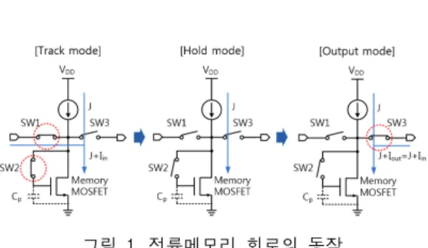
그림 1. 전류메모리 회로의 동작 Fig. 1 Operation of current memory circuit
그림 1은 전류메모리 회로의 동작을 나타낸다. 전 류 Mirror 회로에 입력 전류 및 출력 전류를 제어할 수 있는 스위치와 전류 Mirror 구조를 제어할 수 있 는 스위치를 적용하여, 구성된다. 기본적으로 3개의 스위치로 구성되며 Track, Hold, Output 모드에 의해 메모리 동작을 수행한다[10-12].
(1)
(2)
식 (1), (2)는 스위치 MOS의 기생커패시터 CGD에 의해서 메모리 MOS의 기생커패시터 CGS에 저장된 전압 VGS의 변동을 나타낸다.
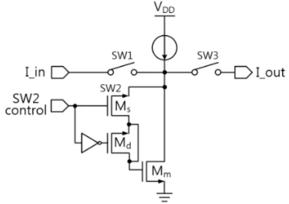
Clock-Feedthrough는 메모리된 Data를 변동시키기 때문에 신호처리 시, 매우 치명적이다. 따라서 Clock-Feedthrough를 최소화하기 위해서 Dummy MOS의 연결이 제안되었다[3],[13].
그림 2는 Dummy MOS를 연결한 전류메모리 회로 를 나타낸다. Dummy MOS는 MOS 커패시터의 동작 으로 Clock-Feedthrough의 원인인 스위치 MOS의 CGD 성분을 최소화시킴으로써 메모리 MOS의 기생 커패시터 CGS에 메모리 되어있는 에너지를 유지할 수 있도록 한다.
그림 2. Dummy MOS를 연결한 전류메모리 회로 Fig. 2 Current memory circuit with dummy MOS
그림 3. Dummy MOS를 이용한 Clock-Feedthrough 최소화 동작
Fig. 3 Clock-feedthrough reduction using dummy MOS transistor
그림 3은 Dummy MOS를 이용하여 Clock-Feedthrough 원인인 스위치 MOS의 기생 커패 시터 CGD의 영향을 최소화하는 개념도를 나타낸다.
이때, Clock-Feedthrough를 최소화하기 위한 동작으 로 메모리 MOS, 스위치 MOS, Dummy MOS의 적정 한 비율의 설계가 필요하다.
부터 Ground까지 두 개의 트랜지스터가 Diode Connection으로 설계되기 때문에 Strong-inversion으 로 전류메모리 회로를 동작시키기 위하여 전원전압은 1.6V 이상으로 인가를 해주어야 한다. 본 설계에서는 전류메모리 회로를 Dynamic Voltage Scaling으로 동 작시키기 위하여 Near-threshold 영역에서의 회로 동 작을 고찰하였다.
식 (3)은 CMOS Inverter 회로 동작에서 나타나는 소비전력을 나타낸다.
(3)
는 Activity factor, 은 Load 커패시터,
는 공급전압, 는 동작 주파수를 의미한다. 위 식에 서 소비전력을 가장 획기적으로 줄일 수 있는 방법은 Square 항인 를 감소시키는 것이다.
이상적으로 Threshold Voltage 이하에서는 Device 가 동작을 하지 않아야 하지만 실제적으로 미세하게 전류가 흐르게 된다. 이 영역의 전원으로 회로를 동작 시킨다면 회로를 초저전력 동작으로 유도할 수 있다.
식 (4)는 Near-threshold 영역에서의 전류식을 나 타낸다.
exp
exp
(4)
(5)
는 Gate 전압, 는 Threshold voltage, 는 Near-threshold slope factor, 는 열 전압, 는 Drain 전압, 는 이동도, 는 Oxide의 커패시터를 의미한다. 이러한 Factor들이 작용하여 Near-threshold 영역에서 전류가 흐르게 된다. 회로의 전원전압을 Near-threshold 영역에서 동작시키게 되 면 회로의 동작이 보장되지 않고 속도에 영향을 받기 때문에 MOS 트랜지스터의 상세한 설계가 필요하다.
그림 4는 Near-threshold 동작의 전류 메모리 회로
그림 4. Near-threshold에서 동작하는 전류 메모리 회로의 전류 측정
Fig. 4 Measurement of current memory circuit with near-threshold
Memory/Switch MOS Width [µm]
Dummy MOS Width [µm]
TP1 [nA]
TP2 [nA]
TP3 [nA]
2 / 0.3 5 26.7 6.63 12.48
2 / 0.3 7 26.7 11.87 16.77
2 / 0.3 9 26.7 16.88 21.37
2 / 0.3 11 26.7 21.04 24.14
2 / 0.3 13 26.7 26.7 26.7
2 / 0.3 15 26.7 32.18 29.85
2 / 0.3 17 26.7 34.04 31.78
2 / 0.3 19 26.7 36.92 34.98
2 / 0.3 21 26.7 38.94 37.01
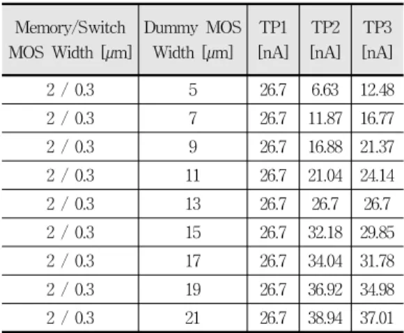
표 1. Dummy MOS 변화에 따른 전류메모리 성능 (sampling 전류 : 26.7nA)
Table 1. The current memory performance according to a change in dummy MOSFET
(sampling current : 26.7nA)
Sampling 주파수는 1MHz로 설계하였고 이에 따라 메모리 Time은 1µs로 설계하였다. 회로의 동작은 1-stage의 전류메모리 회로에서 입력 신호를 Sampling하고 메모리 Time 경과 후에 출력하게 된 다. 다음으로 2-stage 전류메모리 회로에서 1-stage 전류메모리 회로의 출력 전류를 메모리하고 메모리 Time 경과 후에 출력하게 된다. 3-stage 전류메모리 회로에서 또한 2-stage 전류메모리 회로의 출력 전류 를 메모리하고 메모리 Time 경과 후에 출력하게 된 다. 결국 TP1, TP2, TP3에서는 Sampling된 전류를 출력할 수 있게 된다. 표 1은 Dummy MOS Width의 변화에 따른 전류메모리 회로의 성능에 대한 시뮬레 이션 결과를 나타낸다.
그림 5. Dummy MOS Width 변화에 따른 메모리 Error 전류
Fig. 5 Memory error current as a function of Dummy MOS Width
전류메모리 회로에서 바이어스 전류는 90 nA 이고 입력 전류는 26.7nA이다. 표 1의 시뮬레이션 결과로 부터 Dummy MOS의 Width 변화에 따라 메모리 되 는 Data에 변화가 있음을 확인할 수 있었다. Dummy MOS의 Width를 변화시키게 되면 기생 커패시터의 크기가 달라지기 때문에 메모리의 성능에 영향을 주 게 된다. 그림 5는 Dummy MOS Width에 따른 메모 리 회로에서의 error 전류를 나타낸 그래프이다. 메모 리 MOS와 스위치 MOS의 Width는 각각 2µm, 0.3µm 로 고정되었으며, x축은 Dummy MOS의 Width를 나 타내며 y축은 메모리 Error 전류를 나타낸다. 메모리 에러 전류는 [TP2-sampling 전류]의 값과 [TP3-sampling 전류]의 값을 각각 나타낸다. 즉, y축 의 Error 전류가 ‘0’을 가리키면 Clock-feedthrough의 영향이 최소화됨을 의미한다.
표 1과 그림 5로부터 메모리 MOS의 Width를 2µm, 스위치 MOS의 Width를 0.3µm, Dummy MOS 의 Width를 13µm로 설계할 경우, 전류 메모리 회로 의 성능이 저하되지 않고 정상적인 메모리 동작을 수 행함을 확인할 수 있었다.
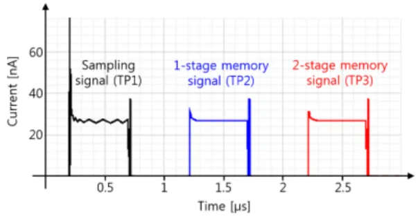
그림 6은 제안한 전류메모리 회로의 시뮬레이션 결 과를 나타낸다. x축은 시간을 나타내며 y축은 전류를 나타낸다. Sampling한 전류가 전류메모리 회로에 의 해 저장되었다가 1µs의 메모리 Time을 갖고 출력됨 을 확인할 수 있었다. 이때, 1.2V의 Near-threshold 전원전압에서 소비전력은 3.7µW으로 계산되었다.
그림 6. Clock-Feedthrough를 최소화한 전류메모리 회로의 시뮬레이션 결과
Fig. 6 Simulation result of current memory circuit with Clock-Feedthrough minimization
그림 7. 근접 임계 전류 메모리 회로 Fig. 7 Circuit of current memory of near-threshold
그림 7은 제작을 위한 Near-threshold 전류메모리 회로 3개의 Layout을 나타낸다. 유효면적은 약 123 µm x 34µm 이다.
Ⅳ. 결 론
본 논문에서는 전류모드 신호처리를 이용한 무선통 신용 LSI의 제작에서 Clock-Feedthrough를 최소화하 는 전류메모리 회로를 제안하고 초저전력 동작이 가 능하도록 Dynamic Voltage Scaling으로 유도하기 위 한 기법을 소개하였다. 0.35µm 공정의 BSIM3 모델을
이용하여 전류메모리 회로를 설계하였고
Near-threshold 영역의 전원전압을 사용하여 시뮬레 이션을 진행한 결과, 전류메모리 회로에서 2µm의 메
3.7µW 으로 계산되었다.
본 연구는 무선통신시스템 회로의 저전력 동작에 유용한 자료가 될 것으로 기대된다.
감사의 글
이 연구는 서울과학기술대학교 교내연구비의 지원으로 수행되었습니다.
본 논문은 한국전자통신학회 가을철학술대회 우수논문으로 선정되었습니다.
References
[1] H. Lee, H. Lee, and H. Shin, “A Study On Ubiquitous Sensor Network Technologies,” J.
of the Korea Institute of Electronic Communication Sciences, vol. 4, no. 1, Mar.
2009, pp. 70-77.
[2] G. Sim and J. Jang, “Design and Implementation of Wireless Multi communication Circuit Based On USN,” J. of the Korea Contents Association, vol. 11, no. 8, Aug. 2011, pp. 33-42.
[3] B. Kim and D. Kim, “Voltage regulator for baseband channel selection filters,” J. of the Korea Institute of Electronic Communication Sciences, vol. 8, no. 11, Nov. 2013, pp.
1641-1646.
[4] C. Lee, S. Lee, and D. Choi, “Communication Module Selection Algorithm for Energy Saving of Smartphone,” J. of the Korea Contents Association, vol. 12, no. 5, May 2012, pp. 22-31.
[5] S. Kim, “Current to Voltage Converter for Low Power OFDM Modem,” J. of the Korea Institute of Electronic Communication Sciences, vol. 3, no. 2, June 2008, pp. 90-96.
[6] Y. Park, J. Min, and S. Hwang, “Current-Mode Serial-to-Parallel and Parallel-to-Serial Converter for Current-Mode OFDM FFT LSI,” The J. of the
Communication MODEM,” J. of the Korea Institute of Electronic Communication Sciences, vol. 3, no. 2, June 2008, pp. 83-89.
[8] G. Balachandran and P. Allen,
“Switched-Current Circuits in Digital CMOS Technology with Low Charge-Injection Errors,” IEEE J. of Solid-States Circuits, vol. 37, no. 10, Oct. 2002, pp. 1271-1281.
[9] M. Goldenberg, R. Croman, and T. Fiez,
“Accurate SI Filters Using RGC Integrators,”
IEEE J. of Solid-States Circuits, vol. 29, no. 11, Nov. 1994, pp. 1388-1395.
[10] Y. Park, S. Hwang, J. Cha, C. Yang, and S.
Kim, “Design of Low-power Serial-to-Parallel and Parallel-to-Serial Converter using Current-cut method,” The J. of Korea Information and Communications Society, vol. 34, no. 10, Oct. 2009, pp. 776-783.
[11] S. Kim, G. Park, and J. Cha, “0.35-μm CMOS-process-based Voltage-to-current Converter Design for an Analog OFDM Device,” J. of Korea Physical Society, vol. 55, no. 1, July 2009, pp. 336-340.
[12] R. Bodnar, “High-Accuracy Current Memory in HV CMOS Technology,” IEEE Trans.
Circuits and Systems II: Express Briefs, vol. 60, no. 6, June 2013, pp. 321-325.
[13] T. Fiez and D. Allstot, “CMOS Switched-Current Ladder Filters,” IEEE J. of Solid-States Circuits, vol. 25, no. 6, Dec. 1990, pp. 1360-1367.
저자 소개
여성대(Sung-Dae Yeo) 2011년 목포해양대학교 해양전자 통신공학부 졸업
2013년 서울과학기술대학교 NID 융합기술대학원 졸업(공학석사) 2013년 ∼현재 서울과학기술대학교 NID융합기술대학원 박사과정
※ 관심분야 : 전류모드 회로 설계, 저전력 회로 설계, 신호처리, 시스템 LSI 설계
김종운(Jong-Un Kim) 2014년 서울과학기술대학교 전자 IT미디어공학과 졸업(공학사) 2014년 ∼현재 서울과학기술대학 교 NID융합기술대학원 석사과정
※ 관심분야 : 전류모드 회로 설계, 저전력 회로 설계, Mixed 회로 설계
조태일(Tae-Il Cho) 2015년 서울과학기술대학교 전자IT미디어공학과 졸업(공학사) 2015년 ∼현재 서울과학기술대학 교 NID융합기술대학원 석사과정
※ 관심분야 : 전류모드 회로 설계, 저전력 회로 설계, 디지털 회로설계, FPGA 프로그래밍
조승일(Seung-Il Cho)
2013년 일본 Yamagata Univ. 이 공학연구과(공학박사)
2013년 ∼현재 일본 Yamagata Univ. Innovation Center for Organic Electronics Assistant Professor
※ 관심분야 : Organic TFT 집적회로 설계, Adiabatic log circuit, 아날로그 디지털 mixed 회 로 설계
김성권(Seong-Kweon Kim) 2002년 일본 TOHOKU대학 대학원 전자공학과(공학박사)
2002년 ∼2004년 일본 TOHOKU 대학 전기통신연구소 Assistant Professor & Research Fellow 2004년 ∼2009년 목포해양대학교 해양전자통신공 학부 조교수
2009년 ∼현재 서울과학기술대학교 전자IT미디어 공학과 교수
※ 관심분야 : 무선통신용 아날로그 LSI 설계