2479
Copyright ⓒ The Korean Institute of Electrical Engineers
This is an Open-Access article distributed under the terms of the Creative Commons Attribution Non-Commercial License (http://creativecommons.org/
Design and FPGA Implementation of FBMC Transmitter by using Clock
Gating Technique based QAM, Inverse FFT and Filter Bank for Low
Power and High Speed Applications
M. Sivakumar
†and S. Omkumar*
Abstract
– The filter bank multicarrier modulation (FBMC) technique is one of multicarrier modulation technique (MCM), which is mainly used to improve channel capacity of cognitive radio (CR) network and frequency spectrum access technique. The existing FBMC System contains serial to parallel converter, normal QAM modulation, Radix2 inverse FFT, parallel to serial converter and poly phase filter. It needs high area, delay and power consumption. To further reduce the area, delay and power of FBMC structure, a new clock gating technique is applied in the QAM modulation, radix2 multipath delay commutator (R2MDC) based inverse FFT and unified addition and subtraction (UAS) based FIR filter with parallel asynchronous self time adder (PASTA). The clock gating technique is mainly used to reduce the unwanted clock switching activity. The clock gating is nothing but clock signal of flip-flops is controlled by gate (i.e.) AND gate. Hence speed is high and power consumption is low. The comparison between existing QAM and proposed QAM with clock gating technique is carried out to analyze the results. Conversely, the proposed inverse R2MDC FFT with clock gating technique is compared with the existing radix2 inverse FFT. Also the comparison between existing poly phase filter and proposed UAS based FIR filter with PASTA adder is carried out to analyze the performance, area and power consumption individually. The proposed FBMC with clock gating technique offers low power and high speed than the existing FBMC structures.Keywords: OFDM, FBMC, Clock gating technique, R2MDC based inverse FFT, UAS based FIR
filter and PASTA adder.
1. Introduction
The Filter bank multicarrier modulation (FBMC) is mainly used in optical communication, wireless communi-cation, Cognitive Radio (CR) network and multiple access networks. FBMC is derived from OFDM with some enhancement in basic structure. The spectral efficiency and data rate is very low in OFDM. Also the power consumption is high and performance is low due to adding cyclic prefix. The FBMC doesn’t required cyclic prefix. So the performance is high and power consumption is very low in FBMC when compared to the OFDM technique. The FBMC is mainly used to transmit a multiple data at a time with multiple carrier frequency. The huge data is transmitted at a time by using either OFDM or FBMC. The large data are divided into multiple subcarriers OFDM. Hence signalling overhead is high and spectral efficiency is low in OFDM. To avoid this kind of issue, non-orthogonal filter bank technique is used in FBMC in order to achieve high spectral efficiency and low signal overhead. However, the complexity is very high in FBMC when compared to
OFDM. To overcome this problem, a lot of structure is introduced to reduce the area utilization and implementation process. Previously, the multi-rate filter or poly phase filter is used to remove the side lobes of FBMC. The area and power consumption is very high in poly phase filter and multi-rate filter. Because this multiplier structure is used in poly phase filter. But currently, the multiplier less FIR filter is introduced in the FBMC technique. Shift and add based multiplication is applied in the recent filter. Hence the complexity is reduced in the recent FBMC structure. Similarly, a new inverse FFT is introduced to reduce the memory size and propagation delay. Also advanced modulation technique is incorporated in FBMC technique to overcome the trade-off between power and speed of FBMC architecture.
2. Existing FBMC Technique
The existing FBMC consists of QAM modulation, Radix2 inverse FFT, parallel to serial converter and poly phase filter as shown in Fig. 1. QAM modulation is used to boost the carrier signal during the data transmission. The 128 point Radix2 IFFT used to convert frequency to time domain. This 128 bit converted to 8 bit by using parallel to serial converter. Finally, the poly phase filter is used to † Corresponding Author: Dept. of Electronics and Communication
Engineering, SCSVMV, India. ([email protected]) * Dept. of Electronics and Communication Engineering, SCSVMV,
India. ([email protected])
removes the side lobes of FBMC transmitter. Hence we can get the clear carrier output.
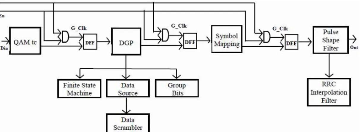
The digital QAM modulation technique consists of QAM trellis code (QAM-tc), data generation and packetization (DGP), symbol mapping and pulse shaping FIR filter as shown in Fig. 2. In the DGP, the whole data are divided into n number of packets and grouping the bits for symbol mapping. In DGP, the controller (FSM) and data source are used to make preamble bit and data bit. The packets are constructed by using scrambling operation of data source. The input data bit stream into six bit integer conversion process is carried out by group bits at 1/6 of sampling rate, as needed by the symbol mapper. In symbol mapping, maps the bits output from DGP to QAM symbols. The up sampling and pulse shaping of symbols is performed by using interpolating root raised cosine (RRC) filter for data transmission.
Fig. 1. Block diagram of Existing FBMC transmitter
Fig. 2. Block diagram of digital QAM modulation
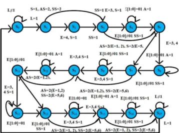
Fig. 3. State diagram of a new proposed booth multiplier
by using add and shift method
The new Moore finite state machine (FSM) is designed to perform booth multiplication based on add and shift to perform both signed and unsigned multiplications as shown in Fig. 3. Hence the area is low and speed is high when compared to all other existing techniques. From the Fig. 3, L is a load word, E=control, AS=add & shift, SS = subtract & shift, A= only addition, S= only subtraction. The output is zero at all the state except S17. In the S17 output is one. The modified radix4 booth recoding technique and a new FSM is used to design a booth multiplier. This booth multiplier register and carry save adder are incorporated into the poly phase filter design [13].
3. Proposed FBMC Technique
The proposed FBMC transmitter contains QAM modulation with clock gating, R2MDC based IFFT with clock gating, parallel to serial converter (PISO) and unified addition and subtraction (UAS) based FIR filter with PASTA adder as shown in Fig. 4. The 64 QAM modulations are performed by combing amplitude modulation and phase shift keying. In digital QAM, the amplitude shift keying is used to convert two digital bit streams. This QAM modulation achieves high data rates by using efficient constellation diagram and linearity of communication channel. The constellation diagram is a representation of signal modulated by a digital modulation scheme. It is used to display the signals as two dimensional XY plane scatter diagram. Type of interference and distortion in a signal is recognized by using constellation diagram measurement. QAM is a higher order of modulation. So it able to carry more bits of data per symbol. The data rate of a link can be increased by selecting high order QAM (64QAM) as shown in Fig. 5. Also clock gating technique is applied in three places of QAM modulation technique in order to reduce power dissipation and optimize the power consumption than the existing QAM modulation.
The circuit diagram of 8point inverse R2MDC FFT with CGT is shown in Fig. 6. From the figure, it consists of butterfly unit (BF), commutator (C2), delay elements (1, 2, 4, 8 bit size), clock gating technique (CGT), diamond shape indicates trivial rotation (odd s) and circle shape denotes non trivial rotation operation (even s). Instead of
pipelined technique, here clock gating technique is applied in the R2MDC IFFT [8] and [9]. The speed is low in radix2 IFFT.
To overcome this problem, the multiple delay element with gate control is used to achieve high speed, low area and low power consumption. Addition, subtraction and multiplication operation is performed in butterfly units. Commutator is used to act as switch to transfer data from one stage to another stage. The –j involves real and imaginary swapping and sign conversion. The clock gating structure is shown in Fig. 7. The system clock and en signal are given to AND gate to produce the gated clock, which is given as clock input of D flip-flops. Hence the clock generation is enabled during active duration. Clock generation is disabled during inactive (hold) condition. Hence it will reduce power dissipation, area and increase the speed of R2MDC FFT.
The unified addition and subtraction (UAS) based common sub expression elimination algorithm is used to design a FIR filter as in Fig. 8. Previously, the multiple
constant multiplications (MCM) based FIR filter is designed by using canonical sign digit (CSD) technique. It consumes more area and power.
To overcome this problem, dual common sub expression (odd and even) algorithm is introduced in UAS technique in order to maximize the computation reuse. The UAS based full adder requires only 3XOR gate and two 2:1
Fig. 5. Block diagram of proposed digital QAM modulation with clock gating technique
Fig. 6. Circuit diagram of inverse R2MDC FFT with clock
gating technique
Fig. 7. Circuit diagram of clock gating technique (CGT)
Fig. 8. Circuit diagram of existing UAS based FIR filter
Fig. 9. Circuit diagram of proposed UAS based FIR filter
MUX [18]. These UAS cells are connected serially to perform unified addition and subtraction operation. Then Shift and add operation is performed to produce the filter output. Further to reduce the power consumption and increase the speed of UAS based FIR filter, the clock gating technique is applied in this structure as shown in Fig. 9.
Also PASTA adder is used instead of RCA [19] and [20]. Recursive parallel asynchronous self time adder is used to remove the hazard, clock skew, Jitter and transition time. Also achieve low area and high speed. The PASTA contains multiplexer, half adder and completion detection unit (NOR gate). Also two state diagrams are used for initial phase and iterative phase. Also reduced half adder and multiplexer are used to design a proposed PASTA adder.
4. Results and Discussion
In this paper, the design of existing and proposed QAM modulation, Existing and proposed IFFT, existing and proposed filter are designed using Verilog HDL language. These three modifications are included in FBMC transmitter structure. Simulation is evaluated by using modelsim 6.3g and synthesize process is carried out by Xilinx ISE 13.2, Virtex5, XC5VLX30 and FF324 devices. Initially, the comparison between existing and proposed QAM modulation is performed to analyze area, delay and power as shown in Table 1. From the results, it shows that the proposed QAM modulation with clock gating techniques offers 1% area reduction, 1% power reduction and 40% delay reduction than the existing QAM modulation.
After that second comparison is performed for both existing and two proposed IFFT as shown in Table 2. The first the comparison between existing radix2 IFFT and pipelined based R2MDC is carried out. From the obtained
results it shows that the pipelined based R2MDC IFFT offers 38.55% area reduction and 1% power reduction than the existing radix2 IFFT. But the delay is increased and speed is decreased. To avoid this problem, the clock gating technique is applied in R2MDC IFFT to achieve low area, delay and power than existing radix2 IFFT. The proposed R2MDC with clock gating technique (CGT) offers 36.64% area reduction 21.13% power reduction and 10.74% delay reduction when compared to existing radix2 IFFT.
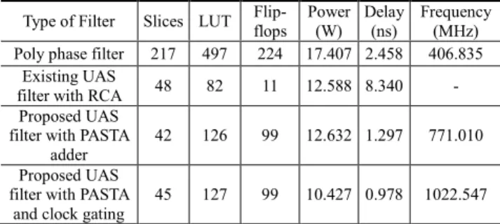
The third comparison is performed between existing and proposed filter as given in Table 3. The proposed UAS filter with Ripple carry adder offers 77.88% area reduction, 27.68% power reduction than the existing poly phase filter. But the delay is very high. To overcome this problem, the proposed UAS filter with PASTA adder is used, which gives 80.64% area reduction, 27.43% power reduction and 47.23% delay reduction than the existing poly phase filter. Further to improve the speed and decrease the delay, the clock gating based UAS filter with PASTA adder is designed. From the results, it denotes that the proposed clock gating based UAS filter with PASTA adder offers 79.26% area reduction, 40.09% power reduction and 60.21% delay reduction than the existing poly phase filter. Finally, these three modifications are included in FBMC transmitter structure.
Comparison between existing and proposed FBMC is performed and the results are given in Table 4. The proposed FBMC without clock gating technique is compared with the existing FBMC transmitter and results says that the proposed FBMC without clock gating gives 5.75% area reduction, 21.86% power reduction and 72.38% delay reduction than the existing FBMC transmitter. Similarly, the proposed FBMC with clock gating technique offers 4.32% area reduction, 32.97% power reduction and 88.03% delay reduction than the existing FBMC transmitter.
Table 1. Comparison between existing and proposed QAM
modulation Type of
Transmitter Slices LUT
Flip-flops Power (W) Delay (ns) Existing QAM 1055 2244 2466 25.732 6.164
Proposed QAM2 with
Clock gating technique 1039 2127 2308 21.726 3.689
Table 2. Comparison between existing and proposed
inverse FFT
Type of IFFT Slices LUT
Flip-flops Power (W) Delay (ns) Frequency (MHz) Existing inverse radix2 FFT 262 695 354 10.425 8.721 114.66 Inverse R2MDC with pipelined FFT 161 443 228 10.368 9.184 108.88 Inverse R2MDC FFT with clock gating 166 444 228 8.222 7.784 128.47
Table 3. Comparison between existing and proposed filter
Type of Filter Slices LUT Flip-
flops Power (W) Delay (ns) Frequency (MHz)
Poly phase filter 217 497 224 17.407 2.458 406.835
Existing UAS
filter with RCA 48 82 11 12.588 8.340 -
Proposed UAS filter with PASTA
adder
42 126 99 12.632 1.297 771.010
Proposed UAS filter with PASTA
and clock gating
45 127 99 10.427 0.978 1022.547
Table 4. Comparison between existing and proposed
FBMC Transmitter Type of
transmitter Slices LUT
Flip-flops Power (W) Delay (ns) Frequency (MHz) Existing FBMC 4186 13658 7802 44.760 23.685 89.047 Proposed FBMC 3945 12745 7370 34.972 3.270 89.047 Proposed FBMC
5. Conclusion
In this paper, low area, low power and high speed filter bank multi carrier (FBMC) transmitter with clock gating technique is proposed by using modified R2MDC based IFFT, modified QAM modulation and UAS based FIR filter with clock gating technique. Simulation is carried out to check the functionality of FBMC transmitter. Synthesis process is performed to evaluate the area, delay and power. FPGA Virtex5 device is used to get the synthesized results of both existing and proposed FBMC transmitter. The proposed inverse R2MDC FFT with clock gating offers 22.83% average area and delay and power product (ADP) than the existing radix2IFFT. Likewise, the proposed UAS based FIR filter with clock gating offers 59.86% average area, delay and power product (ADP) product when compared to the existing poly phase filter. Also the proposed QAM modulation with clock gating offers 14% average area, delay and power product (ADP) product than the existing QAM modulation. Similarly, the proposed FBMC transmitter offers 41.66 average area, delay and power (ADP) product than the existing FBMC transmitter. In future, the MIMO FBMC transmitter/receiver may design for huge data transmission purpose. Also some advanced filter technology is applied for MIMO FBMC transmitter.
References
[1] M. Schellmann et al., “FBMC-based air interface for 5G Mobile: Challenges and proposed solutions,” in Proc. Int. Conf. Cognitive Radio Oriented Wireless Networks (Crowncom), Oulu, Finland, June 2014. [2] S. Rajaram and R. Gayathre, “FPGA Implementation
of Digital Modulation Schemes,” International Journal of Innovative Research in Science, Engine-ering and Technology, vol.3, Special Issue 3, March 2014.
[3] Faiza Quadri and Aruna D., “FPGA Implementation of Digital Modulation Techniques,” International conference on Communication and Signal Processing, IEEE, April 2013.
[4] Akanksha Sinha and Piyush Lotia, “A Study on FPGA Based Digital Modulators,” International Journal of Advanced Research in Electrical, Elec-tronics and Instrumentation Engineering, vol. 4, no. 4, April 2015.
[5] H. Shousheng and M. Torkelson, “A new approach to pipeline FFT processor,” in Proc. Int. Parallel Process. Symp. (IPPS), Apr. 1996, pp. 766-770. [6] Y.N. Chang et al., “An Efficient VLSI Architecture
for Normal I/O Order Pipeline FFT Design,” in IEEE Trans. Circuits Syst. II, vol. 55, no. 12, pp. 1234-1238, Dec 2008.
[7] Kai-Jiun Yang, Shang-Ho Tsai and Gene C. H.
Chuang, “MDC FFT/IFFT Processor With Variable Length for MIMO-OFDM Systems,” IEEE Trans-actions on Very Large Scale Integration (VLSI) systems, vol. 21, no. 4, April 2013.
[8] Mario Garrido, J. Grajal, M. A. Sánchez and Oscar Gustafsson, “Pipelined Radix-2K Feed forward FFT Architectures,” IEEE Transactions on Very Large Scale Integration (VLSI) systems, vol. 21, no. 1, January 2013.
[9] N. Kirubananda sarathy and K. Karthikeyan, “Design of pipeline R2MDC FFT for implementation of MIMO OFDM transceivers using FPGA,” Telecommun Syst, Springer publication, Jan 2016. [10] H. Lin, M. Gharba, and P. Siohan, “Impact of time
and carrier frequency offsets on the FBMC/OQAM modulation scheme,” IEEE Trans. Signal Process. vol. 102, pp. 151-162, Sept 2014.
[11] P. Siohan, Siclet, C., and N. Lacaille, “Analysis and design of OFDM/OQAM systems based on filter bank theory,” IEEE Trans. Signal Process. , vol. 50, pp. 1170-1183, May 2002.
[12] M.Caus and A. Pérez-Neira, “Transmitter-receiver designs for highly frequency selective channels in MIMO FBMC systems,” IEEE Trans. Signal Process. , vol. 60, pp. 6519–6532, Dec. 2012. [13] M.Ramesha and T. Venkata Ramana, “A Novel
Architecture of FBMC Transmitter using Poly phase Filtering and its FPGA Implementation,” Indian Journal of Science and Technology, Vol 9(48), Dec 2016.
[14] Xavier Mestre and David Gregoratti, “Parallelized Structures for MIMO FBMC under Strong Channel Frequency Selectivity,” IEEE Transactions on Signal Processing, vol. 64, no. 5, March 1, 2016.
[15] Jeremy Nadal, Charbel Abde and Amer Baghdadi, “Low-complexity pipelined architecture for FBMC/ OQAM transmitter,” IEEE Transactions on Circuits and Systems-II, vol. 63, no. 1, pp. 1549-7747, Jan 2015.
[16] Doron Gluzer and Shmuel Wimer, “Probability Driven Multi-bit Flip-Flop Integration With Clock Gating,” IEEE Transactions on Very Large Scale Integration (VLSI) Systems, vol. 25, no. 3, March 2017.
[17] Padmini G.Kaushik et al, “Dynamic Power Reduction of Digital Circuits by Clock Gating,” International Journal of Advancements in Technology, vol. 4, no. 1, March 2013.
[18] Jiatao Ding et al, “A New Paradigm of Common Sub-expression Elimination by Unification of Addition and Subtraction,” IEEE Transactions on Computer-Aided Design of Integrated Circuits and Systems, vol. 35, no. 10, Oct. 2016.
[19] M. Sivakumar and S. Omkumar, “Integration of Optimized GDI Logic based NOR Gate and Half Adder into PASTA for Low Power & Low Area
Applications,” International Journal of Applied Engineering Research, vol. 11, no. 4, 2016.
[20] Mohammed Ziaur Rahman et al, “Recursive Approach to the Design of a Parallel Self-Timed Adder,” IEEE Transactions on Very Large Scale Integration (VLSI) Systems, vol.23, no.1, Jan 2015.
M. Sivakumar He received his B.E.
degree in Electronics and Communi-cation Engineering at Sri Chandra sekharendra saraswathi viswamaha Vidyalaya, and the M.E. degree in Anna University, Chennai. He is cur-rently pursuing the Ph.D. degree in Electronics and Communication Engine-ering at Sri Chandrasekharendra saraswathy viswamaha Vidyalaya. His research interests include digital filter design and implementation, CAD algorithms for high-level synthesis and new logical operator design. Filter bank multicarrier, VLSI design, and verification.
S. Omkumar He received PhD Degree
in the area of Communication and networking. His research interests are wireless communication and antennas. He was published around 50 papers in International Journals, National and International Conferences. He is cur-rently working as Associate professor in the department of Electronics and Communication Engineering at Sri Chandrasekharendra Saraswathi Viswamaha Vidyalaya University. He also guest edited several journal special issues and served in several international conferences as advisory and technical program committee.