Study on the Top-Gate Pentacene Thin Film ransistors Using Solution Processing Polymeric Gate Insulator
Gun-Woo Hyung * ․Jun-Ho Kim ** ․Ji-Hoon Seo *** ․Ja-Ryong Koo ****
Ji-Hyun Seo *** ․Jae-Hoon Park ***** ․Young-Ou Jung ******
You-Hyun Kim ******* ․Woo-Young Kim ******* ․Young-Kwan Kim **,✝
* Dept. of Materials Science and Engineering, Hongik University, Seoul, Korea
** Dept. of Electronic Engineering, Hongik University, Seoul, Korea
*** Dept. of Information Display, Hongik University, Seoul, Korea
**** Dept. of Electrical Information and Control Engineering, Hongik University, Seoul, Korea
*****
Dept. of Research Institute of Information Display, Hanyang University, Seoul, Korea
******
Center for Collaborate Instrument, Inha University, Incheon, Korea
*******
School of Display Engineering, Hoseo University, Asan, Korea (Received June 18, 2008 ; Accepted September 12, 2008)
용액 공정 고분자 게이트 절연체를 이용한 Top-Gate 펜타센 박막 트랜지스터에 관한 연구
형 건 우 * ․김 준 호 ** ․ 서 지 훈 *** ․구 자 룡 **** ․ 서 지 현 *** ․ 박 재 훈 ***** ․ 정 용 우 ******
김 유 현 ****** ․ 김 우 영 ****** ․ 김 영 관 **,
* 홍익대학교 신소재공학과, ** 홍익대학교 전기전자공학과, *** 홍익대학교 정보디스플레이공학과
**** 홍익대학교 전기 정보 제어공학과, ***** 한양대학교 디스플레이 연구소
******
인하대학교 기기 분석실, ******* 호서대학교 디스플레이학과 (2008년 6월 18일 접수 ; 2008년 9월 12일 채택)
Abstract : 본 논문에서는 용액 공정을 이용한 고분자 절연층을 갖는 top-gate 구조의 펜타센 박 막 트랜지스터(Thin Film Transistor, TFT)의 특성을 연구하였다. Top-gate 구조의 펜타센 TFT 제작에 앞서 유기 반도체인 펜타센의 결정성 성장을 돕기 위해서 가교된 PVP (cross-linked poly(4-vinylphenol))를 유리 기판 상에 스핀 코팅을 이용하여 형성한 후, 노광 공정을 통해 니켈/은 구조를 갖는 채널 길이 10 ㎛의 소오스, 드레인 전극을 형성하였다. 그리고 열 증착을 이용하여 60 nm 두께의 펜타센 층을 성막하였고, 고분자 절연체로서 PVA(polyvinyl alchol) 또는 가교된 PVA를 용액공정인 스핀 코팅을 이용하여 형성한 후 열 증착으로 알루미늄 게이트 전극을 성막하였다. 이로 써 제작된 소자들의 전기적 특성을 확인한 결과 가교된 PVA를 사용한 펜타센 TFT 보다 PVA를 게이트 절연체로 사용한 소자가 전기적 특성이 우수한 것으로 관찰되었다. 이는 PVA의 가교 공정 에 의한 펜타센 박막의 성능 퇴화에 기인한 것으로 사료된다. 실험 결과 0.9 ㎛ 두께의 PVA 게이트 절연막을 사용한 top-gate 구조의 펜타센 TFT의 전계 효과 이동도와 문턱전압, 그리고 전류 점멸비 는 각각, 약 3.8×10 -3 cm 2 /Vs, -11.5 V, 3×10 5 으로써 본 연구에서 제안된 소자가 용액 공정형 top-gate 유기 TFT 소자로서 우수한 성능을 나타냄을 알 수 있었다.
Keywords : top-gate structure, organic thin-film transistor (OTFT), polymeric insulator.
✝ Corresponding Author (e-mail : [email protected])
1. Introduction
Recently, a tremendous amount of research has been focused on OTFTs (Organic Thin Film Transistors) because they are expected to be one of the most important components to realize low-cost and large-area flexible displays [1,2]. The performance of OTFTs has been improved significantly in the past decade and has already reached a comparable status to hydrogenated amorphous silicon TFTs [3-6]. Most of researches on OTFTs reported up to now have been progressed using the bottom-gate structure. There are two types of source/drain contact configurations in bottom-gate OTFTs, i.e. top and bottom contacts which are generally defined by the position of source/drain electrodes against organic semiconductor.
Bottom-gate TFT employing a top contact structure is rather difficult to fabricate a fine-patterned device due to the shadow effects of metal mask. On the other hand, for the bottom-gate device employing a bottom contact structure, it is difficult to achieve high performance owing to high contact resistance between source/drain electrodes and organic semiconductor layer. However, top-gate OTFTs have advantageous potentials related with elaborate formation of source/drain electrodes by using conventional photolithography processes. In addition, the charge transport along the surface of organic semiconductor film is expected to be more efficient, because of larger grain size with less grain boundaries or trap sites, than that in the bottom of organic semiconductor layer[7]. Therefore, TFTs having a fine channel pattern can be fabricated with a top-gate geometry, thereby providing high performances compared with the bottom-gate devices [8].
Nevertheless, it is not easy to find out the proper gate dielectric materials for the top-gate OTFTs since subsequent processes forming a gate insulator should not degrade
the performance of organic semiconductor layer by organic solvents or thermal treatment for polymerization. Viewed in this light, PVA (polyvinylalchol) is adopted as a gate insulator in this work, which can be prepared without chemical solvents and also polymerized at low temperature below 60°C.
For the fabrication of top-gate OTFTs with pentacene as an organic semiconductor, we have investigated two types of solution processing gate insulators, i.e. PVA and cross-linked PVA. These results are discussed.
2. Experimental
2.1. Fabrication of Top-Gate Pentacene TFTs.
Transistors were fabricated on glass
substrate with device structure as shown in
Fig. 1. Prior to fabricating top-gate pentacene
TFTs, cross-linked PVP (poly(4-vinylphenol))
was prepared by following typical
cross-linking processes [9] and used as a
buffer layer for the crystalline growth of
pentacene molecules in the conducting
channel region. It is observed that the
surface of cross-linked PVP is more
hydrophobic than that of a bare glass
substrate, indicating a lower surface energy
of the buffer layer. Since pentacene film
grown on the substrate having lower surface
energy tends to have a larger sized-grain,
the larger sized-grain of pentacene can be
grown on polymer coated glass substrate
rather than on bare glass substrate. After
buffer layer forming process, 50-nm-thick Ag
film was formed and patterned by
conventional photolithography processes for
source and drain electrodes. The noble
materials such as Au, Pd and Pt have been
recognized as the best metals for the source
drain electrode of pentacene TFTs since
those metals show ohmic contact with
pentacene which can make charge inject
easily from metals into pentacene. However, they are very expensive materials and not easy to pattern by photolithography and chemical process [10]. Therefore, Ag was adopted as source and drain electrode with Ni as an adhesion film for buffer layer and also as a hole injection film to pentacene layer in this work. It is expected that holes are easily injected from the Ni adhesion electrode directly into pentacene by being matched between the work function of Ni and the highest occupied molecular orbital (HOMO) of pentacene. More detail, Ni films with a thickness of 4 nm were thermally evaporated before and after depositing Ag.
After deposition of 60-nm-thick pentacene layer onto the source/drain deposited substrate, 900-nm-thick PVA or 700-nm-thick cross-linked PVA film, as a gate dielectric layer, was formed by spin-coating method. Detailed descriptions on the cross-linking processes of PVA are discussed in other reference[11, 12]. Finally, top-gate pentacene TFTs were constructed by forming Ag gate electrode using a metal shadow mask.
Fig. 1. Schematic of a pentacene thin film transistor structure (top gate).
2.2. Measurements
The current-voltage (I-V) and capacitance- voltage (C-V) characteristics of the fabricated top-gate pentacene TFTs were measured by Keithley 4200 semiconductor analyzer unit and HP-4192 impedance
analyzer, respectively. The morphological characteristics were investigated using atomic force microscope (AFM) (Digital Instruments Nanoscope IV).
3. Results and Discussion 3.1. Analysis of Gate insulators
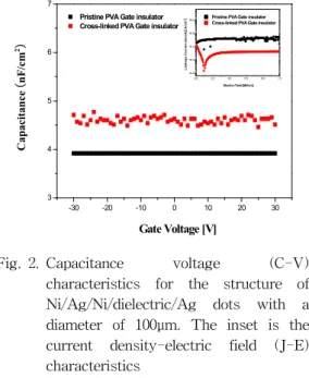
Figure 2 shows the capacitance characteristics of with pristine PVA (900 nm thick) and cross-linked PVA dielectric films obtained from the structure of Ni/Ag/Ni/dielectric/Ag dots with a diameter of 100 μm. Both dielectric films show capacitances of 3.9 nF/cm 2 and 4.5 nF/cm 2 and higher leakage current density ( J~
3×10 -7 A/cm 2 , J~3.9×10 -8 A/cm 2 , see the J-E curve for pristine PVA and cross-linked PVA in the inset, respectively).
-30 -20 -10 0 10 20 30
3 4 5 6 7
Pristine PVA Gate insulator Cross-linked PVA Gate insulator Pristine PVA Gate insulator
Cross-linked PVA Gate insulator
0.0 0.2 0.4 0.6 0.8 1.0
1E-9 1E-8 1E-7 1E-6 1E-5
Electric Field [MV/cm]
Leakage Current density[A/cm2]
Gate Voltage [V]
Capaci ta nc e ( nF /cm
2)
Fig. 2. Capacitance voltage (C-V) characteristics for the structure of Ni/Ag/Ni/dielectric/Ag dots with a diameter of 100μm. The inset is the current density-electric field (J-E) characteristics
3.2. Interface Characteristics
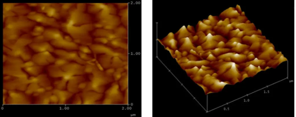
It was found that pentacene molecules
deposited onto the cross-linked PVP buffer
layer were more densely packed and
exhibited a pronounced crystalline growth
compared to those on a bare glass substrate
Fig. 3. Atomic force microscopy AFM images of thermally evaporated pentacene thin films on cross-linked PVP buffer layer
as shown in Fig. 3. Some researches have reported that the crystalline growth of pentacene molecules is strongly correlated with the surface energy of substrates and can be promoted by adopting hydrophobic substrates [13, 14]. Therefore, the larger grain of pentacene film on the buffer layer can be explained by the hydrophobic surface of the cross-linked PVP compared with a bare glass (not shown here).
3.3. Electrical Characteristics of the Thin-Film Transistors
The output characteristics of the fabricated top-gate pentacene TFTs with PVA or cross-linked PVA gate insulator are shown in Fig. 4, where the channel length and width are 10μm and 20μm, respectively. Both TFTs show typical p-type characteristics, while TFT with a pristine PVA gate insulator also exhibited better saturation behavior than device with the cross-linked PVA gate insulator.
Transfer characteristics of our TFTs are also shown in Fig. 5. Considering that OTFTs based on pentacene are operated in the accumulation mode, the saturation drain current (I DS ) can be given by equation (1)
I DS = (W/2L)C i μ fe (V GS -V th ) 2 (1)
where W is the width of the channel, L is the length of the channel, C i is the capacitance per unit area of the gate dielectric, µ fe is the field-effect mobility, Vg the gate voltage and V th is the so-called threshold voltage[10,11]. The mobility is estimated from the slope of a plot of I ds ½
versus V GS . For the device with a bare PVA gate insulator, we have obtained a value of 0.0038 cm 2 /Vs as a saturation mobility and a value of -10 V as a threshold voltage, using the value W/L = 2 and C i = 3.9 nF/cm 2 . The on-off current ratio and subthreshold slope are approximated to be about 3×10 5 and 2 V/decade, respectively, in a gate voltage sweep between 10 and -30 V when the drain voltage V DS set at -10 V, while the device with the cross-linked PVA gate insulator exhibited 3×10 3 and 5 V/decade. Important device parameters are summarized in Table I.
It should be noted that the top-gate
pentacene TFT with the pristine PVA gate
insulator has better field-effect mobility and
on/off current ratio compared to that using
the cross-linked PVA gate insulator. We
believe that the forming condition of PVA
film has induced less damages to the
pentacene active layer than that of
cross-linked PVA film and ammonium
dichromate photosensitizer used for
cross-linking of PVA has detrimentally
(a) (b)
Fig. 4. Ids versus Vds characteristics for a top gate with bottom contact transistor with (a) a cross-linked PVA and (b) a pristine PVA dielectrics.
affected the pentacene film in this work[15].
Consequently, we suggest that the bare PVA can be an efficient candidate for the top-gate pentacene TFTs with high performances.
Further modifications of the fabricating processes and investigations on the interfacial characteristics between pentacene and solution processing polymeric gate insulator in top-gate pentacene TFTs are in progress.
-30 -20 -10 0 10
0.0 5.0x10⁻⁵ 1.0x10⁻⁴ 1.5x10⁻⁴ 2.0x10⁻⁴ 2.5x10⁻⁴
Top gate Vds= -10V
10-13 10-12 10-11 10-10 10-9 10-8 10-7 Pristine PVA Gate insulator Cross-linked PVA Gate insulator