• 검색 결과가 없습니다.

Feasibility of Indium Tin Oxide (ITO) Swarf Particles to transparent Conductive Oxide (TCO)

N/A
N/A
Protected

Academic year: 2021

Share "Feasibility of Indium Tin Oxide (ITO) Swarf Particles to transparent Conductive Oxide (TCO)"

Copied!
4
0
0

로드 중.... (전체 텍스트 보기)

전체 글

(1)

1. Introduction

Recently, industries related to electronics, information and communications have been remarkably advanced in the world.

Those advances are heavily dictated by customer demand. The customers strongly demand the smaller and lighter devices with versatile functionality under considerable price

1)

. With the strong demands, many of indium (In), crucial rare materials, have been used to fabricate the devices. In is widely used for materials of transparent conductive oxide (TCO) as a form of indium tin oxide (ITO) owing to its environmental stability as well as unique high optical transparency and electrical conductivity.

However, the In has been worn off in proportion to growth the In related market such as solar cells, lightings, and displays

2)

. Moreover, electronic wastes are being increasingly emitted from various electronic products. The wastes include ITO target scraps emitted from many factories related to TCO. Although the ITO target scraps is used for recycling of In elements with etching process

3)

, the recycling process generate pollutions

because of hazardous materials containing Cl

-

and NO

3-

elements to dissolve the ITO target scraps into In and Sn under heating conditions

4)

. Following process makes tremendous amounts of wastewater, which is hazardous to air and soil, during synthesis of ITO particles for target. As they are inefficient methods from environmental aspect

5)

, re-use of ITO target scrap instead of conventional recycling process has to be considered to reduce the pollution. Therefore, as a first step, ITO swarf particles obtained from ITO target scarp was characterized after mixing with ITO nanoparticles whether it is feasible to TCO.

2. Experimentals

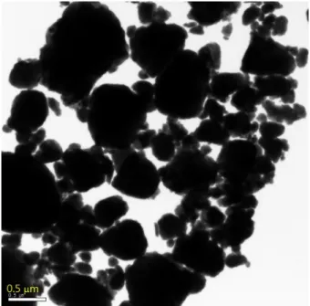
ITO swarf particles were obtained by crashing the ITO target scraps to get fine particles followed by mechanical milling for 4 hours. The ITO particles were observed with a high resolution transmission electron microscope (HRTEM, JEOL, JEM-3010).

The ITO particles were mixed with new ITO nanoparticles with ratio of 3 to 4 by weight. The new ITO nanoparticles were prepared with reported recipe

6)

. The mixture was dispersed into an organic solvent to formulate ITO ink. Concentration of the ITO nanoparticles in the ink was designed as 20 wt%. Thermal

Current Photovoltaic Research 3(2) 50-53 (2015) pISSN 2288-3274

Feasibility of Indium Tin Oxide (ITO) Swarf Particles to Transparent Conductive Oxide (TCO)

Sung-Jei Hong

1)

* ․ DuckJoo Yang

2)

․ Seung Jae Cha

1)

․ Jae-Yong Lee

3)

․ Jeong-In Han

4)

*

1)

Display Components and Materials Research Center, Korea Electronics Technology Institute, Gyeonggi, 463-816, Korea

2)

Department of Chemistry, The University of Texas at Dallas, TX, 75083, USA

3)

Hanchung RF Co. Ltd., Incheon 405-816, Korea

4)

Department of Chemical and Biochemical Engineering, Dongguk University-SEOUL, Seoul, 100-715, Korea

ABSTRACT: Indium (In) is widely used for transparent electrodes of photovoltaics as a form of indium tin oxide (ITO) due to its superior characteristics of environmental stability, relatively low electrical resistivity and high transparency to visible light. However, In has been worn off in proportion to growth the In related market, and it leads to raise of price. Although In is obtained from ITO target scarps, much harmful elements are used for the recycling process. To decrease of harmful elements, ITO swarf particles obtained from target scraps was characterized whether it is feasible to transparent conductive oxide (TCO). The ITO swarf was crushed with milling process, and it was mixed with new ITO nanoparticles. The mixed particles were well dispersed into ink solvent to make-up an ink, and it was well coated onto glass substrate. After heat-treatment at 400°C under N

2

rich environments, optical transmittance at 550 nm and sheet resistance of the ITO ink coated layer was 71.6% and 524.67 Ω /□, respectively. Therefore, it was concluded that the ITO swarf was feasible to TCO of touch screen panel.

Key words: ITO swarf, Target scarp, Ink coated layer, Microstructure, Electrical properties, Optical properties

*Corresponding author: [email protected], [email protected] Received April 7, 2015; Revised April 15, 2015;

Accepted April 17, 2015

ⓒ 2015 by Korea Photovoltaic Society

This is an Open Access article distributed under the terms of the Creative Commons Attribution Non-Commercial License (http://creativecommons.org/licenses/by-nc/3.0)

which permits unrestricted non-commercial use, distribution, and reproduction in any medium, provided the original work is properly cited.

50

(2)

S.J. Hong et al. / Current Photovoltaic Research 3(2) 50-53 (2015) 51

behavior of the formulated ink was analyzed by using a Thermo Gravimetry / Differential Thermal Analyzer (Seiko Exstar 6000, TG/DTA6100). Then, the ink was deposited onto glass substrate by spin coating to obtain thickness of about 1 μm. After deposit, the ITO ink coated layer was heat-treated at the temperature, optimized from thermal analysis, for a 1 hour under inert N

2

rich environments. The characteristics of the ITO layer were evaluated by observing the microstructure, optical and electrical properties with a field emission scanning electron microscope (FESEM, JEOL, JSM6700F), a UV-VIS Spectrophotometer (JASCO, V-560) and a 4-point probe electrical measurement system (Mitsubishi Chemical Analytech, MCP-T610), respectively.

Hall effect measurement system (Ecopia, HMS-3000) was also employed to evaluate the carrier concentration in a magnetic field of 0.55 T at room temperature using van der Pauw method.

3. Results and Discussion

HRTEM observation of the ITO swarf particles is shown in Fig. 1. Particle sizes are widely distributed ranging from 20 nm to 2.7 μm in diameter. The wide distribution is attributed to the large ball size and relatively short time. In order to get fine sized particles, ball size applied to milling process should be decreased

7)

. As ball size decreases, surface area of the ball to be contacted with ITO particles increases. In contrary, as the ball size increases, the contact area decreases leading to coarse-sized particles. Also, as the milling time increases, the particle size

decreases. However, mechanical milling may generate distortion of microstructure such as change in lattice constant

8)

that may affect electrical and optical properties. In this study, to minimize the effect of milling time, milling time was set to 4 hours that is relatively shorter than other works

7,8)

.

Using the ITO particles, ITO ink was formulated by mixing with new ITO nanoparticles with ratio of 3 to 4 in weight. After formulation, thermal behavior of the ink was analyzed. In Fig. 2, the weight of the ink decreases to 20 wt% at around 200°C. Also, the change in heat flow is observed at similar temperature except small change at around 300 to 400°C. This is owing to the thermal decomposition of the organic component out of the ink except ITO particles. That is, the organic components are burnt out of the ink system above the temperature. From the analysis, the heat-treatment temperature expects to be 400°C. Thus, after spin-coating, ITO coated layer was heat-treated at 400°C.

After that, microstructure of the ITO ink coated layer was observed. In Fig. 3, coarse and fine ITO particles were mixed

Fig. 1. HRTEM observation of re-used ITO nanoparticle

Fig. 2. Thermal analysis of ITO ink containing re-used ITO nanoparticles

Fig. 3. Micro-structures of ITO ink layer heat-treated at 400°C

(3)

S.J. Hong et al. / Current Photovoltaic Research 3(2) 50-53 (2015) 52

uniformly. It is originated from the mixture of the milled ITO swarf particles. As the sizes of the ITO particles are larger than those of the newly synthesized ITO nanoparticles, such a microstructure were supposed to generate. In the case of using the ITO swarf particles, the effect of heat-treatment temperature was not remarkable, either. Such a microstructure may cause change in optical and electrical properties of the ITO ink coated layer because the inclusion of coarsened particle increases surface roughness.

Thus, the Hall mobility and concentrations of the ITO ink coated layer was measured. As a result, despite of the coarse particles, Hall mobility of ITO coated layer was measured as 0.667 cm

2

/V. As well, the carrier concentration was measured as 1.381 × 10

20

/cm

3

. The phenomenon is attributed to heat- treatment under N

2

rich atmosphere. That is, the N element affects the electrical properties of the layer. This is related to high crystallity of the ITO swarf particles, i.e., the crystallity of the ITO swarf particle is similar to that of newly synthesized ITO nanoparticles. The similar crystallity minimized the difference in the Hall mobility and carrier concentration. As well, the heat-treatment environment gives high carrier concentration with raised Hall mobility. The high carrier concentration and Hall mobility are predicted to affect the optical and electrical properties.

In Fig. 4, the optical transmittance of the ITO coated layer was 71.6% at 550 nm. This is attributed to carrier concentrations.

That is, high carrier concentration means high oxygen vacancies.

As the oxygen vacancies increased, the defects in the lattice structure also increases and, in result, the optical transmittance penetrating through the ITO lattice decreases. As well, mic-

rostructure may affect the optical transmittance based on surface roughness. That is, the coarse sized particle existing in the ITO ink coated layer inhibits the penetration of visible light resulting in decrease of the optical transmittance. In order to enhance the optical transmittance, the size and morphology of the ITO coated layer has to be improved.

In the case of electrical properties, the sheet resistance of the ITO coated layer was measured as 524.67 Ω /□. This is attributed to high crystallity of the milled ITO swarf particles in addition to newly synthesized ITO nanoparticles. Based on the similar crystallity, mixing of the milled ITO swarf particles improved the electrical properties. It is owing to the improved Hall mobility based on conduction mechanism of hole-electron recombination.

From the results, it is known that the ITO swarf particles affect only optical transmittance, and the optical transmittance may be enhanced by decreasing the particle size and morphology of the ITO swarf particles. Also, with improved optical transmittance, the characteristics showed feasibility to TCO application of touch screen panels.

4. Conclusions

In this study, feasibility of ITO swarf particles on the characteristics of ITO ink coted layer was investigated. The ITO swafr particles of which size ranging from 20 nm to 2.7 μm were obtained from ITO target scraps, and they were well mixed with newly synthesized ITO nanoparticles. The ITO ink coated layer using the mixed ITO particles showed optical transmittance and sheet resistance feasible to TCO. The values of sheet resistance were adaptable to touch screen panel. Therefore, the ITO ink coated layer containing the ITO swarf particles showed feasibility to TCO applications with improved optical transmittance.

Acknowledgments

This study was supported by the Industrial Original Technology Development Program of the Korea Evaluation Institute of Industrial Technology (KEIT) grant funded by the Ministry of Knowledge Economy (No. 10048248).

Fig. 4. Optical transmittance of ITO ink layer heat-treated at

400°C

(4)

S.J. Hong et al. / Current Photovoltaic Research 3(2) 50-53 (2015) 53

References

1. Niittynen, J., Kiilunen, J., Putaala, J., Pekkanen, V., Mäntysalo, M., Jantunen, H., and Lupo, D., “Reliability of ICA attach- ment of SMDs on inkjet-printed substrates”, Microelec. Rel., Vol. 52, Iss. 11, pp. 2709-2715, 2012.

2. Minami, T., “Substitution of transparent conducting oxide thin films for indium tin oxide transparent electrode applications”, Thin Solid Films Vol. 516, Iss. 7, pp. 1314-1321, 2008.

3. Alfantazi, A. M., and Moskalyk, R. R., “Processing of indium:

a review”, Minerals Eng. Vol. 16, Iss. 8, pp. 687-694, 2003.

4. Y. Li, Z. Liu, Q. Li, Z. Liu and L. Zeng, “Recovery of indium from used indium –tin oxide (ITO) targets”, Hydrometallurgy Vol. 105, Iss. 3 –4, pp. 207–212, 2011.

5. Espinosa, N., Garcı´a-Valverde, R., Urbina, A., Lenzmann, F., Manceau, M., Angmo, D., and Krebs, F. C., “Life cycle assess- ment of ITO-free flexible polymer solar cells prepared by roll-to-roll coating and printing”, Solar Energy. Mater. Solar Cell., Vol. 97, pp. 3-13, 2012.

6. Hong, S.-J., Kim, Y.-H., and Han, J.-I., “Development of Ultrafine Indium Tin Oxide (ITO) Nanoparticle for Ink-Jet Printing by Low-Temperature Synthetic Method”, IEEE Trans. Nanotech. Vol. 7, pp. 172-176, 2008.

7. Sendi, R. K., and Mahmud, S., “Quantum Size Effect on ZnO Nanoparticle-based Discs Synthesized by Mechanical Milling”, Appl. Surf. Sci., Vol. 258, pp. 8026-8031, 2012.

8. Can, M. M., Ozcan, S., Ceylan, A., and Firat, T., “Effect of

Milling Time on the Synthesis of Magnetite Nanoparticles by

Wet Milling”, Mater. Sci. Eng. B, Vol. 172, pp. 72-75, 2010.

수치

Fig. 2. Thermal analysis of ITO ink containing re-used ITO  nanoparticles
Fig. 4. Optical transmittance of ITO ink layer heat-treated at  400°C

참조

관련 문서

Indium gallium oxide (IGO) attracts much attention as a key semiconductor for transparent TFT because of its high channel mobility and good optical

“Preparation and properties of transparent conducting indium tin oxide films deposited by reactive evapora- tion”, Thin Solid Films 263 (1995) 105.. [ 8

In order to separate Indium and Tin from spent indium tin oxide (ITO) sludge, direct hydrochloric acid leaching and thermal reduction followed by HCl leaching were applied..

Ramasamy, "Deposition and characterization of indium oxide and indium tin oxide semiconducting thin films by reactive thermal deposition technique",

Abstract This study develops a highly transparent ohmic contact scheme using indium oxide doped ZnO (IZO) as a current spreading layer for p-GaN in order to increase the

Indium tin oxide (ITO) thin films were found in a wide range of optoelectronic applications such as transparent electrical contact electrodes in display, touch screens, thin

Nanosilver on flexible PET substrate is potential materials to replace ITO (indium tin oxide). Protective film is most important to maintain unique silver

Effect of Laser Scanning Speed on the Laser Direct Patterning of T-shaped Indium Tin Oxide (ITO) Electrode for High Luminous AC Plasma Display Panels.. 이조휘 1 , 조의식 1