[발표 1]
LED 발열문제의 근본적 해결을 위한 화학적 리프트오프법
나현석
교사
[발표 2]
OLED 조명의 기술개발과 산어보하 현황 및 전망
박영호
교수
목 차
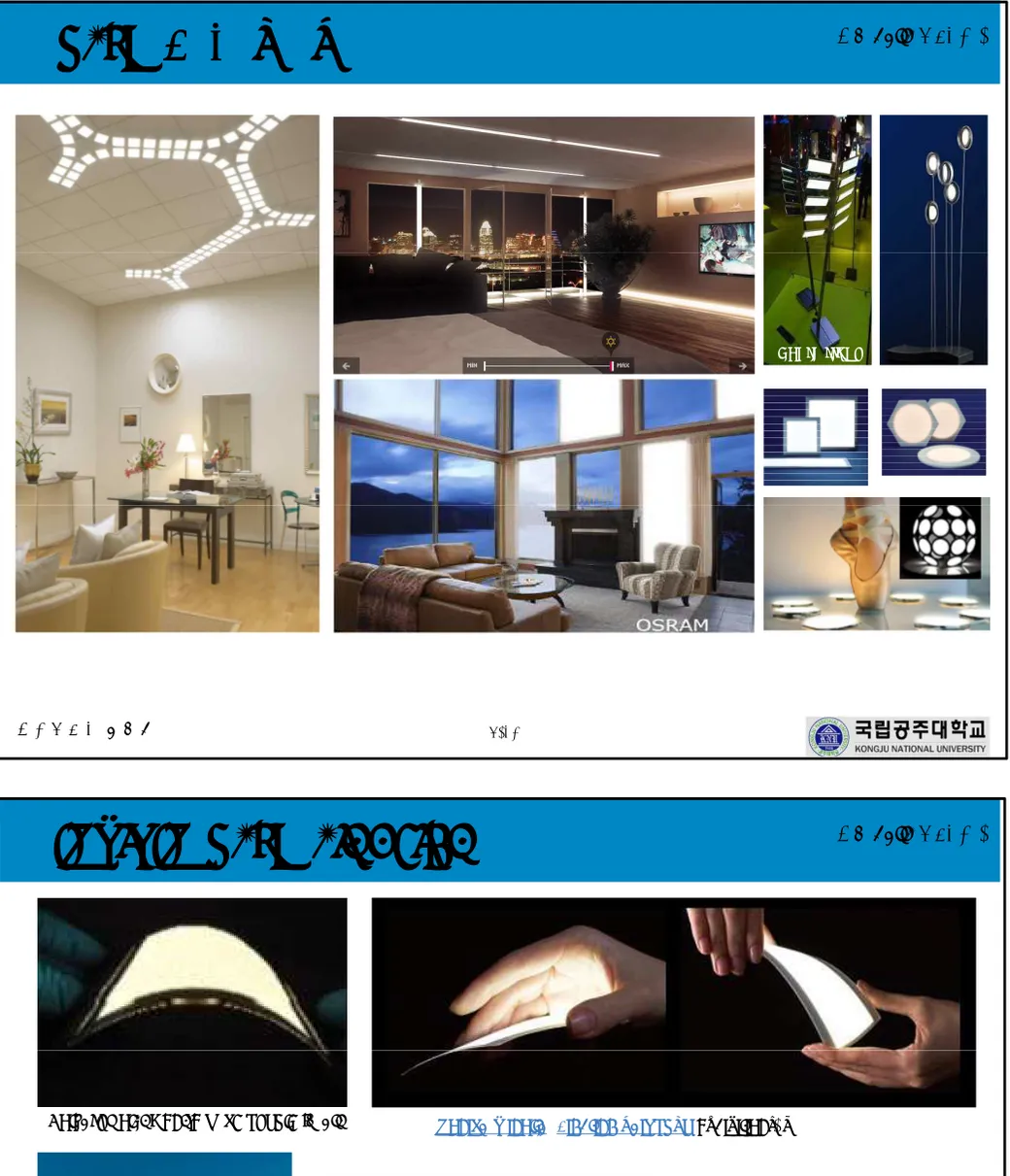
I. What is OLED Lighting?
II. Market Trend of OLED Lighting
III. Technology of OLED Lighting
IV. Application of OLED Lighting
V. Nest Tecnologies of OLED
VI. OLED Modules & Luminaires
I. What is OLED Lighting?
II. Market Trend of OLED Lighting
III. Technology of OLED Lighting
IV. Application of OLED Lighting
V. Nest Tecnologies of OLED
VI. OLED Modules & Luminaires
스마트조명 연구회 2/53
I. What is OLED Lighting?
II. Market Trend of OLED Lighting
III. Technology of OLED Lighting
IV. Application of OLED Lighting
V. Nest Tecnologies of OLED
VI. OLED Modules & Luminaires
OLED 조명 기술개발, 산업화 현황 및 전망
LED, OLED 조명 연구회
OLED 조명 기술개발, 산업화 현황 및 전망
August 15. 2013
History of Display
I. What’s OLED ?
스마트조명 연구회 4/53
Lighting 변천사
I. What’s OLED ?
Proto-Type of Flexible OLED Display
Samsung Emopulse SamsungI. What’s OLED ?
Samsung Emopulse Samsung LG Chem LG Display Samsung 스마트조명 연구회 6/53 Sony UDCOLED Display Applications
I. What’s OLED ?
PM OLED Applications
AM OLED for Smart-Phone
스마트조명 연구회 5/53
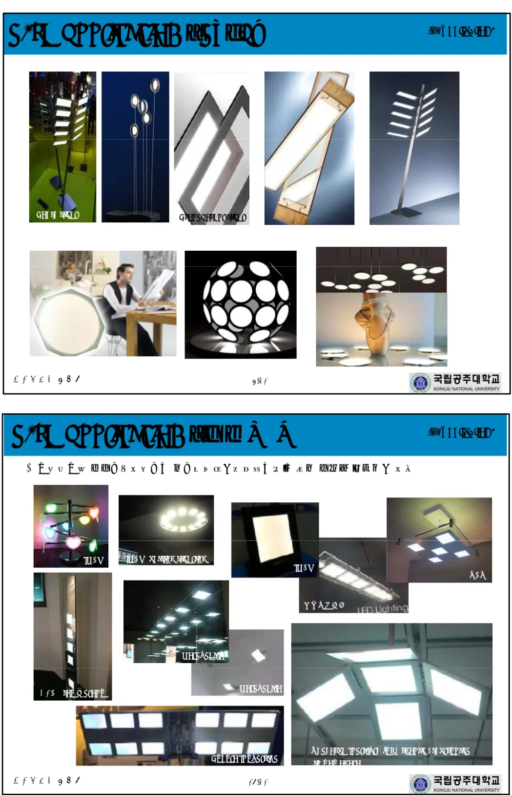
Flexible OLED Lighting
I. What’s OLED ?
Solvay, Holst Centre 69cm2, 30lm/Watt Konica Minolta Lighting Fair 2013exhibition(?)
스마트조명 연구회 8/53
GE and Konica Minolta
flexible desk lamp prototype(2010)
Flex-o-Fab Project(Holst Centre, Philips, DuPont Teijin Films, 2013)
Made by Agfa, Philips and Holst
OLED 조명의 예
I. What’s OLED ?
Table light
기존 조명 산업 현황
II. Market of OLED Lighting
스마트조명 연구회 10/53조명산업 패러다임 전환
ü
에너지 자원의 무기화로 인한 지속적 유가 상승으로 3차 에너지 파동 조짐
ü
교토 의정서(RoHS/WEEE) 발효로 환경 규제 강화
ü
삶의 질 향상으로 인간친화적 감성조명 수요 증가
ü
Display 및 반도체 infra를 이용한 차세대 성장 동력 산업 아이템
ü
미래기술인 Flexible Electronics, 유기전자소자 분야와 핵심 기반 기술 공유 가능
Why OLED Lighting ?
I. What’s OLED ?
q 환경 규제로 백열등 시장이 축소되며, 대체 조명시장으로 LED 및 OLED 조명시장 확대 예상
Lighting Market
II. Market of OLED Lighting
구분 2009 2010 2011 2012 2013 2014 2015 스마트조명 연구회 12/53 근거 : 유비산업리서치 2009 OLED 광원보고서 구분 2009 2010 2011 2012 2013 2014 2015 형광등 42,759 47,694 55,473 61,084 66,695 72,306 77,917 백열등 67,771 69,698 69,437 66,007 62,578 59,149 55,719 LED 1,350 2,000 2,495 3,244 4,217 5,482 7,126
OLED
6
226
432
1,136
1,638
2,902
5,225
전체 111,887 119,617 127,836 131,471 135,128 139,839 145,987Solid State Lighting(고체 조명)
II. Market of OLED Lighting
전세계 광원 시장 전망
-2,000 4,000 6,000 8,000 10,000 12,000 14,000 16,000 20102011201220132014201520162017201820192020 Year M a rke t (M U S $ ) OLED Lighting LED LightingII. Market of OLED Lighting
(단위: 백만 달러, %) 구 분 2012 2014 2016 2018 2020 백열등 2,091 1,543 1,237 828 581 -2,000 4,000 6,000 8,000 10,000 12,000 14,000 16,000 20102011201220132014201520162017201820192020 Year M a rke t (M U S $ ) OLED Lighting LED Lighting 스마트조명 연구회 14/53
출처 : IHS Displaybank Report, “조명용 OLED 산업 분석 및 시장 전망” (July 2012))
구 분 2012 2014 2016 2018 2020 백열등 2,091 1,543 1,237 828 581 형광등 7,776 8,088 7,496 5,988 4,405 할로겐 3,205 3,537 3,471 2,676 1,937 컴팩트 형광등 4,726 5,015 4,208 3,053 2,397 가스 방전등 3,348 3,488 3,341 2,720 1,890 LED 4,098(16.1) 7,582(25.1) 10,804(32.9) 16,857(47.0) 21,476(56.1) OLED 159(0.6) 1,003(3.3) 2,300(7.0) 3,774(10.5) 5,610(14.6) 전체 25,403 30,256 32,856 35,896 38,298
OLED Lighting Market
II. Market of OLED Lighting
② White OLED (Stacked Structure)
① OLED Display (RGB Type)
Cathode
C
a
th
o
d
e
(-)
OLED Display와 OLED Lighting
R
o
w
Anode
III. Tech. of OLED Lighting
・ Matrix Pixels (
R
,
G
,
B
화소형성)
(Crossed Anode & Cathode)・ Line by Line Scanning
・ Discrete ASIC Drivers
(TCP or COG Method)
Anode(+)
Anode
C
a
th
o
d
e
(-)
Column
Cathode
Anode
Pixel
스마트조명 연구회 16/53・ Matrix Pixels (
R
,
G
,
B
화소형성)
(Crossed Anode & Cathode)・ Line by Line Scanning
・ Discrete ASIC Drivers
(TCP or COG Method)
유기물/고분자 ELD
는 반도체 성질을 띄는 유기물 또는 공액 고분자를 발광 소재로 하여 이를 두
전극 사이에 끼워 놓고 전압을 가하면 전류가 발광 소재 내로 흐르면서 유기물 또는
고분자로부터 빛이 발생되는 원리 (
전기발광
이라 부른다)를 이용하는
발광 디스플레이
OLED 발광 원리
III. Tech. of OLED Lighting
Ra≒90
High Color Rendering Index is very important for kind of museum usage because of its own characteristic of the broad spectrum like the sun light.
t:2.22mm & weight:38g
Very thin thickness and light weight are effective for good designing and making new application. Temp:≒30℃
Our OLED lighting panels minimize heat generation & heat influence to irradiated objects. It's suitable for built-in application or museum/food lighting. △u’v’<0.004
chromaticity allowance
Our OLED panel has good deviation in terms of the Energy Star Standard.
Save Energy
Oled panel contribute the reduction of CO2 emission and to save energy than fluorescent lamp in near future.
Hg:zero
Oled panel is mercury free and complied with RoHS. UV:zero
Properties of OLED Lighting
By Panasonic Idemitsu OLED Lighting
III. Tech. of OLED Lighting
Ra≒90High Color Rendering Index is very important for kind of museum usage because of its own characteristic of the broad spectrum like the sun light.
t:2.22mm & weight:38g
Very thin thickness and light weight are effective for good designing and making new application. Temp:≒30℃
Our OLED lighting panels minimize heat generation & heat influence to irradiated objects. It's suitable for built-in application or museum/food lighting. △u’v’<0.004
chromaticity allowance
Our OLED panel has good deviation in terms of the Energy Star Standard.
Save Energy
Oled panel contribute the reduction of CO2 emission and to save energy than fluorescent lamp in near future.
Hg:zero
Oled panel is mercury free and complied with RoHS. UV:zero
스마트조명 연구회 18/53
Ra≒90
High Color Rendering Index is very important for kind of museum usage because of its own characteristic of the broad spectrum like the sun light.
t:2.22mm & weight:38g
Very thin thickness and light weight are effective for good designing and making new application. Temp:≒30℃
Our OLED lighting panels minimize heat generation & heat influence to irradiated objects. It's suitable for built-in application or museum/food lighting. △u’v’<0.004
chromaticity allowance
Our OLED panel has good deviation in terms of the Energy Star Standard.
Save Energy
Oled panel contribute the reduction of CO2 emission and to save energy than fluorescent lamp in near future.
Hg:zero
Oled panel is mercury free and complied with RoHS. UV:zero
OLED Process Sequence (TFT, PM-OLED)
Glass substrate
TFT 구조
AM-OLED
PM-OLED
III. Tech. of OLED
LTPS-Si TFT 공정도
SiO2/a-Si 증착 Interlayer Depo
a ⇒ Poly Si(ELA) Via Pattern (V) Poly-Si Pattern (I) ITO Depo Gate Ox/Metal
증착
ITO Pattern (VI)
Gate Pattern (II) 평탄화막 증착
TFT 구조
AM-OLED
PM-OLED
i) ITO, Cr substrate ii) ITO & Cr Patterningiii) Inter-Insulator formationiv) Cathode separator formation
Array Process : Photo-Etching
Depo & Encap. in OLED Equipment
스마트조명 연구회 17/53
Gate Pattern (II) 평탄화막 증착
이온 주입 평탄화막 Pattern (VII)
SiN 증착
SiN Pattern (III)
S/D Metal 증착 S/D Pattern (IV) LTPS/Oxide TFT 대면적 양산기술확보 ix) Metal Depo x) Encapsulation
xi) Testing xiii) Packaging v) Plasma Treatment vi) HIL/ HTL Depo viii) ETL/EIL Depo vii) R/G/B/W Depo
Future Prospect of OLED Lighting
III. Tech. of OLED Lighting
스마트조명 연구회 20/53
From Panasomic, 2012
Comparison of OLED and LED lighting
OLED 조명의 장점
-. Color Comfort
-. Large-Area Emission
-. Form Factor
OLED 조명의 단점
-. Light Efficiency
-. Lightime
-. Cost Competitiveness
OLED 조명의 장점
-. Color Comfort
-. Large-Area Emission
-. Form Factor
OLED 조명의 단점
-. Light Efficiency
-. Lightime
-. Cost Competitiveness
스마트조명 연구회 19/53IDTechEx Printed Electronics Asia 2013 conference in Tokyo, Japan
OLED 조명 소자의 개발현황
III. Tech. of OLED Lighting
스마트조명 연구회 22/53
Organic LED의 발전 추세
III. Tech. of OLED Lighting
스마트조명 연구회 21/53
OLED Application : 주조명
q 창문의 day/night 활용 비교와 그 외 실내 조명의 예
Day NightV. Next Technology
스마트조명 연구회 24/53 Philips 근거 : OLED 광원기술 및 기술 로드맵_김도근Light Efficiency of OLED Lighting
Panasonic Develops World's Highest Efficiency White OLED for Lighting
Panasonic Corporation today announced that it has developed a white Organic Light
Emitting Diode (OLED) with the world's highest luminous efficiency
*1of
114 lm/W
(light-emitting area of 1 cm²). In addition, a luminous efficiency of 110 lm/W has also
been achieved with a device with a larger emitting area of 25 cm². The panels also
feature long lifetime -
over 100,000 hours
(LT50) and a brightness of of 1,000 cd/m
2.
The panel thickness was less than 2 mm.
•
This development contains the following features:
1. Approximately 2.5 times improvement
*2in the light extraction efficiency (light
extraction efficiency of about 50%)
2. Simultaneous achievement of high efficiency and long lifetime
*3(over 100,000
hours)
•
These features have been achieved with the following technologies:
1. Built-up Light Extraction Substrate (BLES) technology by the optimized
arrangement of the film, glass and air for the suppression of light confinement in
the OLED.
2. Optimal design of stacked organic emitting layers with high-efficiency
phosphorescent materials.
III. Tech. of OLED Lighting
Panasonic Develops World's Highest Efficiency White OLED for Lighting
Panasonic Corporation today announced that it has developed a white Organic Light
Emitting Diode (OLED) with the world's highest luminous efficiency
*1of
114 lm/W
(light-emitting area of 1 cm²). In addition, a luminous efficiency of 110 lm/W has also
been achieved with a device with a larger emitting area of 25 cm². The panels also
feature long lifetime -
over 100,000 hours
(LT50) and a brightness of of 1,000 cd/m
2.
The panel thickness was less than 2 mm.
•
This development contains the following features:
1. Approximately 2.5 times improvement
*2in the light extraction efficiency (light
extraction efficiency of about 50%)
2. Simultaneous achievement of high efficiency and long lifetime
*3(over 100,000
hours)
•
These features have been achieved with the following technologies:
1. Built-up Light Extraction Substrate (BLES) technology by the optimized
arrangement of the film, glass and air for the suppression of light confinement in
the OLED.
2. Optimal design of stacked organic emitting layers with high-efficiency
phosphorescent materials.
스마트조명 연구회 23/53
Panasonic Develops World's Highest Efficiency White OLED for Lighting
Panasonic Corporation today announced that it has developed a white Organic Light
Emitting Diode (OLED) with the world's highest luminous efficiency
*1of
114 lm/W
(light-emitting area of 1 cm²). In addition, a luminous efficiency of 110 lm/W has also
been achieved with a device with a larger emitting area of 25 cm². The panels also
feature long lifetime -
over 100,000 hours
(LT50) and a brightness of of 1,000 cd/m
2.
The panel thickness was less than 2 mm.
•
This development contains the following features:
1. Approximately 2.5 times improvement
*2in the light extraction efficiency (light
extraction efficiency of about 50%)
2. Simultaneous achievement of high efficiency and long lifetime
*3(over 100,000
hours)
•
These features have been achieved with the following technologies:
1. Built-up Light Extraction Substrate (BLES) technology by the optimized
arrangement of the film, glass and air for the suppression of light confinement in
the OLED.
Applications of OLED Lighting (LG Chem)
스마트조명 연구회 26/53
From LG화학 Homepage
Lighting Source of OLED Lighting (LG Chemical)
해외 OLED 조명업체의 Roadmap (II)
IV. Applications
스마트조명 연구회 28/53
“OLED 조명 기술 동향” in 전자통신동향분석 제24권 제6호 2009년 12월
해외 OLED 조명업체의 Roadmap (I)
IV. Applications
스마트조명 연구회 27/53
q 야마나시현 산업기술진흥기구 유기일렉트로닉스연구소와 여러 업체가 공동으로 진행
OLED Application : 일본의 예
IV. Applications
IMES-ceiling lighting IMES 고이즈미산업 IMES Matsushita NEC 스마트조명 연구회 30/53
Research Institute for Organic Electronics in Yamagata
OLED lamp stand Matsushita
Toyota Industries
OLED Application : OSRAM
IV. Applications
Table light Transparent light
OLED Product Roadmap : DOE SSL
V. Next Technology
스마트조명 연구회 32/53
Properties of Panasonic Idemitsu OLED Lighting
What’s Process to Down the Manufacturing Cost.
OLED Price Projection
OLED Price Projection
Cost w/ Method
Cost w/ Method
스마트조명 연구회
Sample OLED Manufacturing Cost Roadmap.fromWilliam Feehery, DuPont, “OLED Lighting Manufacturing Cost,” SSL Manufacturing Workshop, Fairfax, VA, April 2009
<Ref. : DOE SSL> Sample OLED Prince Roadmap.
OLED Lighting in OLED100.eu-project
14 partners from 6 countries
Develop all the necessary technologies forming the basis for efficient OLED applications
for the general lighting industry in Europe
Equipment : R&D & Mass Production
V. Next Technology
스마트조명 연구회 36/53
From Sunic System Ltd.
1. Process Chamber
& Vacuum System
-. Chamber
-. Mechanical Pump
-. High Vac. Pump
-. Gate V/V
-. Shutter
2. Aligner
-. CCD Camera
-. Lens
-. Lighting
-. PC w/ Grab Board
-. Shadow Mask
3. Evaporation Cell
-. Host Cell
-. Dopant Cell
-. Power Supplier
4. Thickness Control System
-. Crystal Sensor
-. Sensor Head
-. Thickness Controller
Organic Evaporation System
CCD
Glass
Mask
Shutter
THK
Monitor
Sensor
Cell
MotorAligner
PVD(물리 기상 증착)공정의 정의는 생성하고자 하는 박막과 동일한 재료(Al, Ti, TiW, W, TiN, Pt 등)의
입자를 진공 중에서 여러 물리적인 방법에 의하여 기판 위에 증착시키는 기술을 말한다. PVD중 여러가지
열원에 의해 증착하고자 하는 물질의 증발 현상을 이용한 증착 방식을 evaporation(진공증발증착)이라 한다.
V. Next Technology
1. Process Chamber
& Vacuum System
-. Chamber
-. Mechanical Pump
-. High Vac. Pump
-. Gate V/V
-. Shutter
2. Aligner
-. CCD Camera
-. Lens
-. Lighting
-. PC w/ Grab Board
-. Shadow Mask
3. Evaporation Cell
-. Host Cell
-. Dopant Cell
-. Power Supplier
4. Thickness Control System
-. Crystal Sensor
-. Sensor Head
-. Thickness Controller
Cryo
Pump
CCD
Glass
Mask
Shutter
THK
Monitor
Sensor
Cell
G/V
THK
Sensor Cont’r MotorThickness
Monitor
스마트조명 연구회 35/531. Process Chamber
& Vacuum System
-. Chamber
-. Mechanical Pump
-. High Vac. Pump
-. Gate V/V
-. Shutter
2. Aligner
-. CCD Camera
-. Lens
-. Lighting
-. PC w/ Grab Board
-. Shadow Mask
3. Evaporation Cell
-. Host Cell
-. Dopant Cell
-. Power Supplier
4. Thickness Control System
-. Crystal Sensor
-. Sensor Head
-. Thickness Controller
Mechanical
Pump
CCD
Glass
Mask
Shutter
THK
Monitor
Sensor
Cell
Host Dopant
THK
Sensor Cont’rCell
Vacuum System
u
u
G5 OLED
G5 OLED 조명
조명 장비
장비 In
In –
– Line System Concept
Line System Concept
((공동
공동 Project DMS + Sunic System+ SNU)
Project DMS + Sunic System+ SNU)
[LLB]
GLS
[LMC]
Moving
GLS
[Chuck] OC Mask Return MC Mask Return
White OLED용 inline Type 장비
V. Next Technology
[LL]
[MS]
[Loader]
GLS
[Port#1]
[BF#1] [OC#1] [OC#2] [OC#3] [BF#2] [PMC] [BF#3] [MC] [BF#4][Port#2] [Un-loader]
[MS]
5G OLED 조명 장비 사진
Items
Unit
Dev. Target
Glass size
Gen.
5
Tact Time
min
< 1
스마트조명 연구회 38/53
Tact Time
min
< 1
Depo. Rate
Å·m/min
≥ 600
O-Efficiency
%
≥ 60
O-Thick Non-Unif
%
≤ ± 2
Depo. Rate
Å·m/min
≥ 1,000
Metal Thick. Non-Unif
%
≤ ± 5
Continuous Depo. Time
hr
≥ 300
OLED System Full Layout for Display
-. Multi-Process Loading to Un-Loading
-. Real-Time Process & H/W Control
-. Low Particle Technology
-. High Vacuum Control(<1E-8 Torr)
-. Long Time Reliability
-. Minimum Working Time (> 144hr)
V. Next Technology
-. Multi-Process Loading to Un-Loading
-. Real-Time Process & H/W Control
-. Low Particle Technology
-. High Vacuum Control(<1E-8 Torr)
-. Long Time Reliability
-. Minimum Working Time (> 144hr)
Roll-to-Roll OLED Fabrication
V. Next Technology
스마트조명 연구회 40/53
GE Flexible Lighting Prototype
Deposition Equip. of R2R at Vacuum
V. Next Technology
Top Level의 R&D Activity
Ceramic Layers Isolation LayersGlass Substrate
Barix coating Active OLEDBarix T/F Encap. in Vitex Co.
V. Next Technology
스마트조명 연구회 42/53
System Configuration for Barix Encap.
Ref. http://www.vitexsys.com
Encapsulation of OLED
1. Metal or Glass
CAN
Glass substrate
V. Next Technology
OLED Requirement Limit of MOCON measurement
2. Glass or Polymer
Sheet
Glass substrate
Glass substrate
Glass/Polymer
Water Permeation Rate (g/m
2/day at 25
℃
) in T/F Encapsulation
스마트조명 연구회 41/53
10-6 10-4 10-2 100 102 104
H
2O permeation Rate (g/m
2/day at 25℃)
ETRI(2003.4) OLED Requirement P E C V D In o rg a n ic C o a tin g O rg a n ic C o a tin g s P E T ( h a rd -c o a t) P N B ,A rt o n
3.
Thin Film
Passivation
OLED Display/Lighting에 대한 Supply Chain
Substrate
-Glass
- Flexible
ITO, Metal
Insulator
Organic
Materials
-Host
-Dopant
Barrier,
Encap
Equipment
- Backplane
- Evaporation
- Encapsulation
OLED Lighting
1) TFT 기판(Display) Patterned ITO(조명) 기판제조
Panel Manufacturing
2) OLED 증착
3) Encapsulation
OLED Display, Lighting Design/Manufacturing
스마트조명 연구회 44/53
Consumer / User
높은 에너지 효율, 환경/인간 친화적, Design Freedom을 가진 Display와 조명
반도체, 디스플레이 Infra를 OLED 산업으로
Distributor (B to C)
System Integrator (B to C)
Improved Efficiency by Light Extraction
• External outcoupling is limited to extraction of light trapped in
glass substrate (substrate modes)
• Only internal outcoupling allows the extraction of the trapped
light inside the active OLED layers (organic modes)
• Combination of internal and external outcoupling gives the
best results
• External outcoupling is limited to extraction of light trapped in
glass substrate (substrate modes)
• Only internal outcoupling allows the extraction of the trapped
light inside the active OLED layers (organic modes)
• Combination of internal and external outcoupling gives the
best results
스마트조명 연구회 43/53
No outcoupling
OLED
OLED
External outcoupling foil
Internal outcoupling and
external outcoupling foil
OLED Modules
OPTICS
Highest optical lighting quality and
efficacy in combination with
a high quality surface
The optimal combination regarding optics, mechanics and electronics
OPTICS
Highest optical lighting quality and
efficacy in combination with
a high quality surface
MECHANICS
Optimized and robust
contact system integrated in
a slim format
스마트조명 연구회 46/53
MECHANICS
Optimized and robust
contact system integrated in
a slim format
ELECTRONICS
Efficient converter program out of one hand
Supply Chain에 따른 경쟁력
Items
Sub-Items
International
Domestic
Substrate
(기판)
- Glass
- Flexible
- Corning, ISAHI,
- FUJI Film, Vitex, etc
-. 삼성코닝, LG Chem. etc
Anode & Insulator
(전극 및 절연)
- ITO, Metal
- Insulator
- Ulvac, Kuramoto,
Geomatec
- 희성 금속
- 신안 SNP
- ITO, Metal
- Insulator
- 희성 금속
- 신안 SNP
Organic
Layer (유기증착)
- Host
- Dopant
Idemitsu Kosan, Merck,
Eastman Kodak, UDC,
Dupont, CDT, Novaled
LG화학, 두산전자, SFC,
덕산하이메탈, Dow Chemical,
대주전자
Encapsulation
(봉지)
- Barrier
- Encapsulation
Schott, Dynic Nagase
Vitex, Philips,
Nanonics, Novatec, 모디스텍
Equipment
(장비)
- Backplane
- Evaporation
- Encapsulation
- Module 및 측정장비
Tokki, Ulvac,
미쯔비시중공업, Applied
Materials
DMS, SEMES, KC-Tech
Sunic, SFA, YAS,
IM Tech, ADP,
SNU, McScience,
스마트조명 연구회 45/53- Backplane
- Evaporation
- Encapsulation
- Module 및 측정장비
DMS, SEMES, KC-Tech
Sunic, SFA, YAS,
IM Tech, ADP,
SNU, McScience,
OLED Lighting
Panel (광원)
- AMOLED Panel
- Lighting Panel
Osram, Philips, GE, 코니카
미놀타, 루미오텍, Tohoku,
파니소닉 정공
LG Chem., 삼성 SMD, 네오뷰
코오롱
Lighting Extraction
(광추출)
- Internal
- External
Schott, NALUX, 3M, ASAHI,
Anteryon
MTN, Kolon, etc
OLED Lighting
Fixture (조명)
Motivation of smart lighting developments
LED and OLEDs could cut power consumption by 50% by 2025.
Optimization and innovation for greater energy efficiency. 10-15% energy savings through improvements in efficiency with no change in design. Lighting management permits energy savings of up to 80%: § Daylight-based control: 40-60% § Presence detectors: 15-30%
Modern lighting concepts can achieve savings of up to 20%.
Project sequence: § Consulting § Visualization of dynamic lighting scenarios using the Vivaldi software package Electronic ballast
technology is a prerequisite for intelligent lighting management systems.
Light source
Luminaire
Lighting-management
Lighting
concept
Converter
스마트조명 연구회 48/53 Optimization and innovation for greater energy efficiency. 10-15% energy savings through improvements in efficiency with no change in design. Lighting management permits energy savings of up to 80%: § Daylight-based control: 40-60% § Presence detectors: 15-30%Modern lighting concepts can achieve savings of up to 20%.
Project sequence: § Consulting § Visualization of dynamic lighting scenarios using the Vivaldi software package
Only the optimisation of all components results into the best energy lighting solution
OLED Luminaires/on the Light+Building 2012
Application Efficiency – Illuminance Patterns
• Application efficiency =
Theoretical lumens /
Actual lumens
• OLED system
improves application
efficiency by 18-93%
over existing systems.
• OLEDs at 60 lm/W
matches
fluorescents at 100
lm/W in terms of
lighting power
density.
2x4’ fluorescent troffer
Recessed, 8’ x 10’ on center
Cluster of OLED panels
Variable Placement Density
• Application efficiency =
Theoretical lumens /
Actual lumens
• OLED system
improves application
efficiency by 18-93%
over existing systems.
• OLEDs at 60 lm/W
matches
fluorescents at 100
lm/W in terms of
lighting power
density.
스마트조명 연구회 50/53• Application efficiency =
Theoretical lumens /
Actual lumens
• OLED system
improves application
efficiency by 18-93%
over existing systems.
• OLEDs at 60 lm/W
matches
fluorescents at 100
lm/W in terms of
lighting power
density.
From Mike Lu, Jeannine Fisher, and Peter Ngai. Acuity Brands Lighting Inc.
OLED Integration Aspects
Standarized light
sources
Optimized
Converter
Conventional
OLED
OLED
Light source
OLED
Converter
)Lamp
OLED
Module
Technical reasons
- Limited area possible
in fabrication
- Current requirements
for large areas
- Lighting homogeneity
requirements
- Yield in fabrication
Business reasons
-Yield related costs
- Higher volume due to
standarized sizes
스마트조명 연구회 49/53
June 7th 2011
Luminaire
Technical reasons
- Limited area possible
in fabrication
- Current requirements
for large areas
- Lighting homogeneity
requirements
- Yield in fabrication
Business reasons
-Yield related costs
- Higher volume due to
China in LED Industry.
스마트조명 연구회 52/53
William E. Quinn of Veeco, SSL 2012
OLED 조명 산업 핵심역량 강화로 조기 산업화
□ OLED 분야의 기술이 대기업 위주로 편성
ㅇ 국책 과제가 주로 대기업 주도로 이루어짐.
ㅇ 중소기업 R&D 자금 확보의 어려움.
ㅇ 장비와 장비의 부품간 세제 지원 차별
□ OLED분야 산업기반센터의 활용이 어려움.
ㅇ OLED관련 산업기반센터가 작은 규모로 흩어져 있어 유기적 협력네트워크 구축 필요
* 관련센터: 전북나노센터(프린팅), 광주나노센터(OLED장비), 포항나노센터(소재/소자),
서울대유기디스플레이연구센터(공정/소자) 등
□ 신 사업 분야의 조기 사업화 전략 필요 : 4~5세대급 테스트 장비 Infra 구축
ㅇ 국책사업에 의한 특허 활성화/중소기업 활용도 향상 방안 마련
ㅇ 산업화 기술 개발이 절실함. (Low Cost 제조 기술)
- 현재 구축된 장비로는 재료평가, 소자 평가만 가능함.
조기 산업화를 위하 4~5 세대급 평가 라인 구축 및 활용 방안 마련
ㅇ OLED 조명에 대한 응용 방안 마련
- OLED 조명 Design House/차세대 조명 상설 전시관
□ OLED 조명 보급화사업
ㅇ 광원의 특성을 감안한 시범 건물 구축
ㅇ LED와 동등 수준의 보급화 사업 추진
□ OLED 조명관련 연계 기술 확보
ㅇ 부품, 소재, 장비, 차세대 기술 등에 대한 연계 Project
스마트조명 연구회 51/53□ OLED 분야의 기술이 대기업 위주로 편성
ㅇ 국책 과제가 주로 대기업 주도로 이루어짐.
ㅇ 중소기업 R&D 자금 확보의 어려움.
ㅇ 장비와 장비의 부품간 세제 지원 차별
□ OLED분야 산업기반센터의 활용이 어려움.
ㅇ OLED관련 산업기반센터가 작은 규모로 흩어져 있어 유기적 협력네트워크 구축 필요
* 관련센터: 전북나노센터(프린팅), 광주나노센터(OLED장비), 포항나노센터(소재/소자),
서울대유기디스플레이연구센터(공정/소자) 등
□ 신 사업 분야의 조기 사업화 전략 필요 : 4~5세대급 테스트 장비 Infra 구축
ㅇ 국책사업에 의한 특허 활성화/중소기업 활용도 향상 방안 마련
ㅇ 산업화 기술 개발이 절실함. (Low Cost 제조 기술)
- 현재 구축된 장비로는 재료평가, 소자 평가만 가능함.
조기 산업화를 위하 4~5 세대급 평가 라인 구축 및 활용 방안 마련
ㅇ OLED 조명에 대한 응용 방안 마련
- OLED 조명 Design House/차세대 조명 상설 전시관
□ OLED 조명 보급화사업
ㅇ 광원의 특성을 감안한 시범 건물 구축
ㅇ LED와 동등 수준의 보급화 사업 추진
□ OLED 조명관련 연계 기술 확보
Artificial Lighting in All of the World
스마트조명 연구회 53/53
[발표 3]
OLED 조명용 패널의 고효율화 기술 및 응용 기술
유병곤
박사
OLED 조명 개요
Ⅰ
Ⅲ
Ⅱ
Ⅳ
V
OLED 조명 개발 현황
ETRI Technology Portfolio
무선제어 OLED 조명 시스템
Light Extraction Technology
Outline
VI
Summary
1
OLED Research Team / Byoung-Gon Yu
OLED 조명용 패널의 고효율화 기술
및 응용 기술
스마트 조명 지식연구회 발표자료
OLED Research Team / Byoung-Gon Yu
1. OLED 조명 개요
– OLED 기술을 기반으로 한 친환경, 에너지 절감형 차세대 조명 기술 – 우수한 색감, 높은 연색성을 가질 뿐만 아니라 초박형 평판광원으로 디자인의 우수성을 갖는 감성조명 기술전통조명
면조명
투명조명
플렉서블조명
OLED 조명의 특징
3OLED Research Team / Byoung-Gon Yu
1. OLED 조명 개요
전자
수송층
(ETL)
발광층
(EML)
정공
수송층
(HTL)
양극
(투명전극, ITO 유리, 등)음극
(낮은 일함수 금속, Ca, Al:Li, Mg:Ag,등)-
전자
정공
+
-
+
두께: 100 ~ 200 nm
Exciton
1) Carrier Injection (balanced injection; N
e= N
h)
2) Carrier Transport (bipolar transport;
m
e=
m
h)
3) Electron-hole recombination and exciton formation
1. OLED 조명 개요/
OLED Research at ETRI
1. Artistic
2. Transparent
3. Color Tunable
4. Flexible OLEDs
A. Various OLED panels
C. Design contest
D. IEC OLED Lightings Section
Dr. D.-H. Cho
Convener of OLED lighting section
B. Light extraction
5
OLED Research Team / Byoung-Gon Yu
1. OLED 조명 개요
Osram
Aston Martin One-77 supercar
OLED Research Team / Byoung-Gon Yu
2. OLED 조명 개발 현황
7
OLED Research Team / Byoung-Gon Yu
1. OLED 조명 개요/
OLED Research at ETRI
E. Interactive OLED
2. OLED 조명 개발 현황
효율
OLED 조명용 유기소재
고효율
백색 소자/패널 기술
광추출
소재/공정
OLED 면광원 구동 회로
수명
유기소재/소자/구동
방열봉지 소재/공정/장비
가격
OLED 면광원 생산 장비
저가격 패터닝 공정 및 장비
OLED 면광원 등기구
모듈
등기구/디자인
400 500 600 700 800 0.0 0.2 0.4 0.6 0.8 1.0 Peak, FWHM BD (473, 56) GD (510, 61) RD (600, 58) N orma lize d In te nsi ty (a .u .) Wavelength (nm) 디스플레이용 발광소재 디스플레이용 발광소재를 이용한 백색광의 연색성 400 500 600 700 800 -0.2 0.0 0.2 0.4 0.6 0.8 1.0 1.2 1.4 1.6 1.8 Wavelength (nm) No rm ali ze d I nte ns ity ( a.u .) BD:GD:RD=1:1:1 WOLED 1 CRI 74 9OLED Research Team / Byoung-Gon Yu
OLED Research Team / Byoung-Gon Yu
3. ETRI Technology Portfolio
OLED 조명 Value Chain
유리/소재/부품 OLED 면광원 Electronics 조명
Internal Light Extraction Films
Enhancement
> 50 %
High Refractive Index Films
N > 1.7
For micro pattern &
nano pattern
11
OLED Research Team / Byoung-Gon Yu
3. ETRI Technology Portfolio
OLED 조명 Value Chain
유리/소재/부품 OLED 면광원 Electronics 조명
White OLED devices
-
Phosphorescence
- 형광/인광 Hybrid
- Tandem structure
- Transparent & Flexible
- Color Tunable
효율 (lm/W) 형광/인광 Hybrid Phosphorescence
single
Tandem
single
Tandem
Flat27
@ 1000 nit @ 3000 nit
25
@ 1000 nit50
@ 3000 nit34
Transparent
20
@ 1000 nit @ 1000 nit
40
Flexible
30
@ 3000 nitColor
Tunable Color 패터닝된 패널 대비 80% 이상의 효율 Transparent & non-Transparent Stack 형
* @ ~ 3000 K, ~ 80 CRI
3. ETRI Technology Portfolio
OLED 조명 Value Chain
유리/소재/부품 OLED 면광원 Electronics 조명
OLED panels
with artistic grid
Transparent OLED panels
Lighting Window
Color Tunable OLED panels
13
OLED Research Team / Byoung-Gon Yu
3. ETRI Technology Portfolio
OLED 조명 Value Chain
OLED Research Team / Byoung-Gon Yu
3. ETRI Technology Portfolio
OLED 조명 Value Chain
유리/소재/부품 OLED 면광원 Electronics 조명
공진형 무선전원 OLED 조명
송신모듈
수신모듈
15
OLED Research Team / Byoung-Gon Yu
3. ETRI Technology Portfolio
OLED 조명 Value Chain
4. Light Extraction Technology
χ : out-coupling coefficient
η
int: internal quantum efficiency
Radiation mode : ~20%
Glass waveguide mode : ~ 35%
ITO/organic waveguide mode : ~45%
OLED 고효율화
내부 양자효율 (internal quantum efficiency) 향상
- 고효율 소재
- 고효율 소자
광추출 효율 향상
•내부 광추출 기술
•외부 광추출 기술
17OLED Research Team / Byoung-Gon Yu
3. ETRI Technology Portfolio
OLED 조명 Value Chain
유리/소재/부품 OLED 면광원 Electronics 조명
OLED Research Team / Byoung-Gon Yu
4. Light Extraction Technology
OLED의 광추출 기술은 기판과 공기 사이의
전반사 효과에 의한 손실을 줄이기 위한 외부
광추출 기술과 기판과 OLED 소자의 박막 사
이의 wave-guiding 효과에 의한 손실을 줄이
기 위한 내부 광추출 기술로 구분할 수 있음.
외부 광추출 기술은 비교적 안전하고 용이하
게 광추출 효율을 높일 수 있는 기술이나 광
효율의 향상이 50% 정도로 한계가 있음.
내부 광추출 기술은
이론적으로 3배 이상의
광효율 향상을 보일 수 있는 있으나 매우 민
감하게 내부 OLED 구조에 영향을 주므로 전
기, 기계, 화학적 특성을 모두 만족해야 하는
난이도가 높은 기술임.
기술 개발의 필요성
19OLED Research Team / Byoung-Gon Yu
4. Light Extraction Technology
※ Loss due to wave-guided mode :
4-1. Light Extraction Technology
기술의 특징
• Cost Effective Process (Photoless Nano Random Patterning)
• Scalable Technology
• OLED 내부 광추출 효율 향상
Nano random pattering W/O Photolithography
Random 마스크 형성 기판 etching 마스크 제거
고굴절 평탄층 코팅 OLED 제조
Planarization layer w/ high refractive indexy
21
OLED Research Team / Byoung-Gon Yu
OLED Research Team / Byoung-Gon Yu
4-1. Light Extraction Technology
on Flat Glass (E-1 Glass) on Nano-structured Glass (NS-Glass)
-굴절률 ; > 1.9
-투명 ; > 90%
-후막 ; 500~1,000nm
-박리 ; X
-황변 ; X
-후공정정합성 ;
. Ra = 2.5 ~ 6.0nm . ITO증착 damage free 300 400 500 600 700 800 900 1000 0.0 0.2 0.4 0.6 0.8 1.0 1.2 1.4 1.6 1.8 2.0 2.2 2.4 n of HPL1 k of HPL1 n & k Wavelength / nm 300 400 500 600 700 800 50 60 70 80 90 100 Transm ittance ( % ) Wavelength (nm) Flat Glass/HPL1 E1-Glass/HPL1 NS-Glass/HPL1Planarization with high n
23
OLED Research Team / Byoung-Gon Yu
Plastic substrate preparation process
4-2. Light Extraction Technology
Wrinkles?
A small ridge or furrow especially when formed on a surface by the
shrinking or contraction
of a smooth substance.
(Merriam Webster) The formation of wrinkles is a stress involved mechanical process.
The presence of compressive stress across the surface is the main cause of wrinkle formation. Thermodynamically, the formation of wrinkle is an effort of the system to minimize its free energy.
Ref) E. Cerda and L. Mahadevan, Phys. Rev. Lett. 90 (2003) 74302 Geometry and Physics of Wrinkling
?
Mega scale
Nano scale25
OLED Research Team / Byoung-Gon Yu
4-1. Light Extraction Technology
OLED Research Team / Byoung-Gon Yu
4-2. Light Extraction Technology
Spin coating UV exposure Wrinkle formation
OLED light extraction Wrinkle characterization
Experimental approach
Our experimental approach for forming wrinkles consists of only two-steps.
1) liquid prepolymer was spin-coated to form an organic thin film.
2) organic thin film was cross-linked by a UV exposure process.
SEM, AFM, Transmittance and Haze
OLED fabrication: vacuum process
Bottom emission OLED with phosphorescent green (~ 540nm)
Processing scheme
27
OLED Research Team / Byoung-Gon Yu
4-2. Light Extraction Technology
Synthesis of liquid prepolymer
Substrate
Liquid prepolymer
t
t
UV
In the UV process, the moieties form chemical binding to form a solid entity. Compressive stress (t) acts on the
prepolymer during the UV curing process to cause wavy patterns on the film
Wrinkle formation
Liquid prepolymer : transparent and water like
The prepolymer molecule has two crosslinking moieties.
Stress induced wrinkle formation
2000 rpm 3000 rpm 4000 rpm 5000 rpm
50 mm 50 mm 50 mm 50 mm
Wrinkle size is controllable.
Thinner films are easily perturbed.
Controllable transmittance and haze ( Wide applicability)
or RPM
Film thinkness
Wrinkle size
, Transmittance
4-2. Light Extraction Technology
Characteristics of wrinkles
29
OLED Research Team / Byoung-Gon Yu
4-2. Light Extraction Technology
The length of the wrinkles has a range of 10~ 16
m
m,
and two or three wrinkles are extending in the same
direction. In the Fourier transformation space(Inset), no
distinct diffraction pattern, spot or ring, was observed,
indicating the absence of long range ordering.
The optical transmittance of the wrinkle film on the
glass was ~ 15%. The measured haze was 94 %,
indicating optical scattering of nearly all incident light.
The AFM image captures the three dimensional shape
of wrinkles. The height and the pitch were measured as
860 nm and 1.55
m
m, respectively. Wrinkles appear
owing to the presence of stress in the crosslinking
process. Because there is no preferred stress release
direction wrinkles develop randomly.
OLED Research Team / Byoung-Gon Yu OLED with wrinkle film show enhanced
luminance. ( Constant J condition)
Size effects of wrinkle light extraction
Higher light extraction in high viewing angle
Max. 60% enhancement
Negligible angle dependency on EL spectra
4-2. Light Extraction Technology
Light extraction using wrinkles
31
OLED Research Team / Byoung-Gon Yu
4-2. Light Extraction Technology
Wrinkle as light extractor in OLED application
Glass Anode (ITO) Organics Cathode
Wrinkles of can reduce total internal reflection
and contribute in light extraction(Substrate/Air)
a) Attachable wrinkle film
b) Wrinkle film attached on OLED
a) b)
Fabrication of attachable wrinkle film
Attachable wrinkle films were fabricated.
Highly flexible
Easily scalable
5. 무선제어 OLED 조명 시스템
• ETRI OLED House
- OLED + Smart functional - Color tunable, dimming
- Space embedded – emotional lighting - Android smart control
- Ambient wireless sensor
시연 시스템
•
ETRI 색가변 OLED 광원 이용
•
미니어처 하우스 제작
•
하루의 변화에 따라서 조명 환경의
변화를 시연
33OLED Research Team / Byoung-Gon Yu
5. 무선제어 OLED 조명 시스템
OLED Driver AC/DC Converter DC/DC Converter Bluetooth Transceiver ZigBee Transceiver MCU Wireless Sensors OLED Driver OLED Driver OLED Driver OLED Driver DriverOLEDOLED Driver OLED Lamp 사용자 입력 구동정보 , 환경 정보 센싱정보 OLED Lighting Driving System
Wireless sensors Tablet : User interface
OLED Research Team / Byoung-Gon Yu
5. 무선제어 OLED 조명 시스템
4.0 4.5 5.0 5.5 6.0 6.5 7.0 7.5 0 50 100 150 200 Cu rren t (mA) Volatge (V) Wireless Driving DC Driving유무선으로 구동된 OLED
광원의 IV특성
정류된 무선 전원 OLED의
Turn-on 특성
정류된 무선 전원 OLED의
구동 특성
공진형 무선 전원 공급 및 OLED 조명 모듈의 구동 특성
•
공진형 무선 전원 공급 OLED 조명은 무선 전력 전송 수신부로부터 정류된
직류 전원을 공급받아 OLED 광원이 점등하게 됨. 수신부에는 정류회로를
포함하고 있어 안정적인 직류를 공급하게 되며, 이로부터 OLED 광원은 유
선 전원 공급과 동일한 Diode 특성을 나타냄.
기술의 특징
35OLED Research Team / Byoung-Gon Yu
5. 무선제어 OLED 조명 시스템
기술의 특징
1130 cd/m2 1010 cd/m2 1220 cd/m2 1180 cd/m2 1090 cd/m2 복수의 공진형 무선 전원 공급 OLED 조명 모듈
•
함수발생기, 전력증폭기, 자동 임피던스 매칭기를 무선전력전송 송신부의
파워코일에 연결하여 전력을 전송함. 무선 전력 전송 수신부, 정류기, 퓨즈
는 PCB 기판에 일체화 되어 있으므로 무선 전력 전송 수신부와 OLED 조명
을 연결함으로써 복수의 OLED 모듈을 구동할 수 있음.
37OLED Research Team / Byoung-Gon Yu
OLED Research Team / Byoung-Gon Yu
Acknowledgement
•Funding
This work was supported by ETRI R&D Program(The title of research project : “Development of interactive smart OLED lighting technology ") funded By the Government of Korea
ETRI R&D supporting program of MKE/KEIT (Development of Light and Space Adaptable Display)
•OLED research center members
Dr. Seung Koo Park, Mr. Joohyun Hwang, Dr. Jin Woo Huh, Mr. Jin-Wook Shin, Mr. Jun-Han Han, Mr. Chul Woong Joo, Dr. Jonghee Lee, Dr. Doo-Hee Cho, Dr. Nam Sung Cho, Dr. Jong Tae Lim, Ms. K. -I. Song, Ms. S. J. Lee, Dr. Hye Yong Chu, Dr. Byoung-Gon Yu, Dr. Jeong-Ik Lee(Leader)
39
OLED Research Team / Byoung-Gon Yu