P2-60 / S. Choi
• IMID 2009 DIGEST
Dielectric Thin Film
Using Atmospheric Pressure Plasma Polymerization
Sunglan Choi, and Hongdoo Kim*
Dept. of Display Materials Engineering, Kyung Hee Univ., Gyungkido 449-701, Korea
Tel.:82-31-201-2446, E-mail: [email protected]
Keywords: OTFT, atmospheric pressure plasma, dielectric layer
Abstract
The atmospheric pressure plasma polymerization of acrylate monomers was carried out to have dielectrics with easy preparation and high performance. The effects of discharge power, monomer concentration and deposition time on film properties were investigated using various characterization tools. With proper conditions, smooth dielectric layer of 100nm thickness was obtained. Dielectric property as organic dielectric layer has been studied for future applications in organic thin film transistors(OTFT).
1. Introduction
The plasma polymerization in a low pressure gas plasma leads to the formation of polymeric materials.[1] This unique technique to fabricate thin films has been used in a wide variety of applications including barrier coatings and dielectric layer in electronics.[2] Recently, new atmospheric plasma polymerization has been developed and did not requires vacuum chamber to generate thin films. One of current issues on display industry is how to make the product easy and cheap. This new method may fulfill the requirement of process and expand toward various application on display industry such as flexible panel, coating etc.. In this study, we examined the properties of plasma polymerized materials on Si wafer as well as polymer substrate. Furthermore, to test dielectrics, OTFT was prepared and its performance was compared with other known polymer gate insulator.
2. Experimental
Plasma-polymerized methyl methacrylate (MMA) was deposited under the following various experimental conditions such as discharge power (10~500W), monomer concentration and deposition time. MMA monomer was kept in the bubbler system. Flowing Ar gas will deliver MMA monomer vapor into atmospheric plasma region where the plasma polymerization will take a place. Film thickness can be controlled by changing the deposition time and the resulting morphology of the film was checked by either AFM or FE-SEM.
For OTFT device fabrication, top-contact Au electrodes were deposited by thermal evaporation. Pentacene as organic semi- conductor was thermally deposited on dielectric-coated Si substrate at a rate
of 0.01~0.05nm/s. The OTFT output (Ids vs Vds) and
transfer (Ids vs Vgs) characteristics were measured
using probe station(Agilent 4156C).
3. Results and discussion
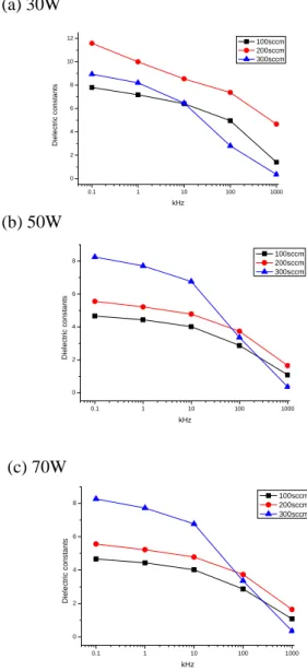
Figure 1 shows the variation of dielectric constants as function of frequency for atmospheric plasma-polymerized PMMA film at different discharge powers. Most of gate dielectric layers require characteristics including high-permittivity or dielectric constants, barrier properties to prevent tunneling, stability, good interface quality and good
film morphology.
[3]
We investigated the electricaland chemical properties of plasma-polymerized thin film used as a gate dielectric layer. The substrates in this experiment were used doped Si wafers and ITO-coated glasses. Film thickness at varying conditions
P2-60 / S. Choi
IMID 2009 DIGEST •
was found to be from 50nm to 600nm. The dielectric constants for plasma-polymerized PMMA and
spin-coated PMMA film were compared using the
Si/PMMA/Au structure.
(a) 30W
(b) 50W
(c) 70W
Figure 1. Dielectric constants of plasma polymerized PMMA films. The discharge power at (a) 30W, (b) 50W, and (c) 70W.
Figure 2. FE-SEM images of deposited films with various thickness: (a) 100nm, (b) 200nm, (c) 350nm, and (d) 600nm.
The several types of plasma films compared to the spin-coated PMMA films. The general trends are similar to each other, but, the absolute values of dielectric constant were different. This may reflect that the compositions of plasma polymerized PMMA and conventional PMMA are different due to severe polymerization condition of plasma polymerization. Figure 2 shows the surface morphology at the different thickness. Thin film shows very smooth surface morphology whereas thick film becomes rough characteristics. Figure3 shows the electrical properties of pentacene OTFT. In the case of plasma-polymerized MMA as gate insulator, the electric characteristics of pentacene OTFT were
obtained with mobility of 0.019 cm2/Vs, Ion/Ioff ratio
~104.
(a) output curve (b) transfer curve
Figure 3. Electrical characteristics of the OTFT : (a) output curve, (b) transfer curve.
0.1 1 10 100 1000 0 2 4 6 8 10 12 Di el ect ri c co nst ant s kHz 100sccm 200sccm 300sccm -60 -50 -40 -30 -20 -10 0 -2.0x10⁻⁶ -1.5x10⁻⁶ -1.0x10⁻⁶ -5.0x10⁻⁷ 0.0 5.0x10⁻⁷ ID VD 0 -60 -40 -30 -20 -10 0 10 20 1E-10 1E-9 1E-8 1E-7 1E-6 VG logI ID I 0.0000 0.0001 0.0002 0.0003 0.0004 0.0005 0.0006 0.0007 0.0008 SQ R T II DI 0.1 1 10 100 1000 0 2 4 6 8 Di el ec tr ic co ns ta n ts kHz 100sccm 200sccm 300sccm 0.1 1 10 100 1000 0 2 4 6 8 D ielec tric c onst ants kHz 100sccm 200sccm 300sccm
P2-60 / S. Choi
• IMID 2009 DIGEST
4. Summary
We investigated the electrical properties of plasma polymerized MMA thin film as OTFT gate dielectric layer. The plasma-polymerized PMMA thin films showed higher dielectric constants than conventional PMMA, which may reflect chemical composition difference in detailed structure. The atmospheric plasma polymerization may be an effective method to deposit thin films compared to the conventional polymers and be applied to organic electronics such as gate insulator, solution-free shadow mask patterning, large area deposition and low-cost process.
Acknowledgements
This work was supported by Gyungkido Regional Research Center (GRRC) fund of Gyungkido, Korea.
5. References
[1] H. Biederman, and Y. Osada, Plasma
Polymerization Process, Plasma Technology,
vol. 3, Elsivier (1992)
[2] T. Kasih, S. Kuroda, and H. Kubota, Plasma
Processes and Polymers, 4, pp648-653 (2007)
[3] B.C.Yoo, S. C. Gong, I. S. Shin, and H. J.
Chang, Journal of the Semiconductor &
Display Equipment Technology, 4, pp69-73