Single Crystalline NbO2 Nanowire Synthesis Bull. Korean Chem. Soc. 2012, Vol. 33, No. 3 839 http://dx.doi.org/10.5012/bkcs.2012.33.3.839
Single Crystalline NbO
2Nanowire Synthesis by Chemical Vapor Transport Method
†Sunghun Lee, Hana Yoon, Ilsun Yoon,a and Bongsoo Kim*
Department of Chemistry, KAIST, Daejeon 305-701, Korea. *E-mail: [email protected] Received December 9, 2011, Accepted December 29, 2011
We report for the first time the synthesis of niobium dioxide nanowires on a sapphire substrate by chemical vapor transport method. We identified single crystalline nature of as-synthesized nanowires by scanning electron microscopy and transmission electron microscopy. Niobium dioxide nanowires with their large surface-to-volume ratio and high activities can be employed for electrochemical catalysts and immunosensors. The Raman spectrum of niobium dioxide nanowires also confirmed their identity.
Key Words : NbO2, Nanowires, Single crystal, Vapor transport, Raman spectrum
Introduction
Transition metal oxides show interesting properties such as superconductivity, piezoelectricity, and magnetoresistance.1 These materials can be industrially employed in lithium-ion battery, catalysis, sensors, and device interconnectors.2-7 The synthesis of single crystalline transition metal oxide nanowires (NWs) attracts particular interest because of their possible applications as highly sensitive and selective catalysts, high performance lithium ion batteries, and highly efficient solar cells, since the contact between active material and electrolyte becomes excellent due to a large surface-to-volume ratio of the NWs.8-10 The good crystallinity and high aspect ratio of the transition metal oxide NWs are favorable for electron transport and could allow faster kinetics and higher sensitivity than the bulk or thin films.9
Among transition metal oxides, niobium (Nb) oxides are applied in resistors in superconducting circuits, electrochemical catalysts, electrochromic films, and oxygen sensors.11-14 Elec-trical properties of Nb oxides are strongly dependent on the oxidation number of Nb.15,16 NbO crystal with a defective NaCl structure shows high room-temperature conductivity, a metallic behavior, and shows superconducting transition at 1.6 K.11,17 Nb2O5 is the most stable Nb-oxide and has excellent dielectric properties.18 NbO2 with a distorted rutile structure is an n-type semiconductor with a small band gap of 0.5 eV at room temperature, showing semiconductor-metal transition at 1081 K.19
Recently, electrochemical electrodes based on Nb/NbO2
for electrochemical immunosensors, which can be applied in biotechnology, pharmaceutical industry, and clinical diagnostics, have been reported.20 Nb/Nb oxides may become a good candidate for the biosensors that can directly monitor antigen-antibody complex or biotin-avidin complex structures by detecting impedance change. Exploiting their chemical stability
in an acid solution, NbO2 nanoparticles are used for high activity Pt/NbO2/C electrocatalysts, which is employed in proton exchange membrane fuel cell for oxygen-reduction reaction, largely increasing mass activities of electrocataly-sts such as Pt or Pb.21,22
Here, we report for the first time the synthesis of single crystalline NbO2 NWs with a very small diameter. While synthesis of Nb2O5 NWs have been reported,23,24 there is no report on the synthesis of single crystalline NbO2 NWs so far despite their excellent electrochemical and electrical pro-perties. Our as-synthesized NWs show highly single crystalline nature, as analyzed by transmission electron microscopy (TEM) and selective area electron diffraction (SAED) patterns. Raman spectrum indicates the vibrational mode peaks of NbO2 NWs ensemble. Raman investigation of nanomaterials is effective for the in-situ nondestructive studies of both the crystallinity and phase transitions of metal oxide nanostruc-tures.25 Single crystalline NbO2 NWs with a very small diameter are one of the promising candidates for impedimetric immunosensors and expected to enhance the electrocatalytic activity in fuel cells.
Experimental Section
Single crystalline NbO2 NWs were synthesized on a c-cut sapphire substrate in a horizontal two-zone furnace equipped with a 1-inch diameter quartz tube as shown in Figure 1. The temperatures of two zones were independently controlled for the vaporization of precursors and the nanostructure growth. Anhydrous NbCl5 powder (0.1 g, 99.95%, metal basis, Alfa
Aesar) in a small alumina boat was used as a precursor and placed in the upstream (US) zone. A c-cut sapphire substrate was located ~10 cm away from NbCl5 precursor at the
downstream (DS) zone. No catalyst was employed. The US and DS zones were heated up to and maintained at 520 K and 1170 K, respectively for 40 min. The quartz tube was evacuated and then purged by argon (Ar) for 20 min to eliminate oxygen. NbCl5 precursor was evaporated at 520 K
and transported onto the substrate by Ar carrier gas at a flow rate of 100 standard cubic centimeters per minute (sccm). No
†This paper is to commemorate Professor Kook Joe Shin's honourable retirement.
aPresent address: Department of NanoEngineering, University of Cali-fornia, San Diego, La Jolla, CA 92093, USA
840 Bull. Korean Chem. Soc. 2012, Vol. 33, No. 3 Sunghun Lee et al.
vacuum pump was used and the pressure was maintained at 1 atm. The formation of NbO2 NWs is ascribed to the
reaction of NbCl5 vapor with oxygen supplied by diffusion
from the atmosphere into the reaction chamber.
As-synthesized NbO2 NWs were analyzed with a Philips
XL30S field emission scanning electron microscope (FE-SEM). X-ray diffraction (XRD) patterns of as-grown NWs were obtained by a Rigaku D/max-rc (12 kW) diffractometer at 30 kV and 60 mA with a Cu Kα radiation source. Trans-mission electron microscope (TEM) images, high-resolution TEM (HRTEM) images, and selective area electron diffraction (SAED) patterns were taken on a JEOL JEM-2100F at 200 kV. Elemental composition of NbO2 NWs was studied by
energy-dispersive X-ray spectrometry (EDS) attached to the TEM. Raman spectrum was measured with a home-built micro-Raman system based on an Olympus BX41 microscope. The 633 nm radiation of a He-Ne laser (Melles Griot) was used as an excitation source and the laser light was focused on a sample through a ×100 objective (numerical aperture NA = 0.7, Mitutoyo).
Results and Discussion
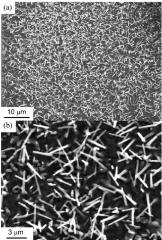
Figure 2(a) shows the FE-SEM image of NbO2 NWs
syn-thesized on a c-cut sapphire with high density. Diameters of the NWs ranging from 20 to 40 nm and lengths up to few micrometers are observed. A magnified SEM image (Figure 2(b)) reveals that the NWs have straight morphology and a clean surface. No secondary growth or extra structural feature is observed. Figure 3 shows an XRD pattern of as-grown NbO2 NWs on a sapphire substrate. The entire diffraction
peaks are indexed to the tetragonal phase of NbO2 with
lattice parameters of a = b = 0.9693 nm and c = 0.5985 nm (space group I41/a, JCPDS card no. 44-1053).
To characterize the crystal structure and elemental com-position of the NWs, we carried out the TEM, HRTEM, and EDS analyses. A representative TEM image in Figure 4(a) shows that NbO2 NW has a diameter of ~20 nm. The SAED
pattern obtained from the NW (inset in Figure 4(a)) reveals single crystalline nature of the NW and can be fully indexed to the tetragonal NbO2 structure down to the [010] zone axis.
NbO2 NW grows along the [001] direction. Repeated TEM
and SAED measurements for several NWs exhibited identical results. Figure 4(b) shows an HRTEM image of NbO2 NW
with clear lattice fringes, again confirming single crystalline
nature of the NW. The lattice spacing of the planes is mea-sured to be 0.2571 nm, agreeing well with the spacing of the (202) planes of tetragonal NbO2 structure. The two-dimensional
fast Fourier transform (FFT) pattern of the lattice-resolved image (inset in Figure 4(b)) obtained from a white square part in the HRTEM indicates that the reciprocal lattice fringes are also matched with the tetragonal NbO2 structure.
Figure 4(c) shows the TEM-EDS line profile spectrum taken
Figure 1. Experimental setup for NbO2 NW synthesis. The temper-atures of two zones are independently controlled.
Figure 2. (a) Representative FE-SEM images of NbO2 NWs grown on a sapphire substrate. (b) A magnified FE-SEM image of NbO2 NWs.
Figure 3. XRD pattern of as-synthesized NbO2 NWs. All of the peaks are indexed to tetragonal β-NbO2 (space group I41/a, JCPDS card no. 44-1053).
Single Crystalline NbO2 Nanowire Synthesis Bull. Korean Chem. Soc. 2012, Vol. 33, No. 3 841
from NbO2 NW. The composition of Nb and O elements in
the NW is approximately 1:2. The line profile reveals that the intensities of peaks due to Nb and O elements, respect-ively, increase toward the center of the NW.
We suggest two possible growth mechanisms of NbO2
NWs as following; first, Nb metal nanoparticles formed by condensation of Nb atoms on a sapphire substrate originated from the precursor molecules may act as a catalyst, inducing vapor-liquid-solid (VLS) growth of NbO2 NWs. SEM image
(Figure 2(b)) and TEM images, however, do not show the presence of any metal catalyst on the NW tip. Hence, VLS growth via Nb metal catalysts is unlikely. Second, NbO2 NWs
may grow spontaneously on the preformed NbO2 thin film
via self-seeded growth. Note that NbO2 NWs are synthesized
on the thin film as shown in Figure 2(b). Considering XRD data that exhibits only peaks for the tetragonal NbO2 phase,
the thin film is probably composed of tetragonal NbO2
crystals. From the observation of NbO2 thin film grown on a
sapphire substrate, we hypothesize on the growth mechanism of NbO2 NWs. After the formation of NbO2 thin film at the
initial stage of reaction, NbO2 NWs epitaxially grow on the
thin film surface by self-seeded growth. Generally, the degrees of supersaturation in a conventional chemical vapor deposi-tion (CVD) system become higher in the beginning of precursor evaporation and get lower as the reaction proceeds. Similar film formations in the growth of Nb2O5 and ZnO
NWs have been reported.23,26
The formation of NbO2 NWs can be explained by two
plausible reaction pathways. NbCl5 powder is evaporated in
the US zone, in which NbCl5 vapor is formed at a
tempera-ture of about 520 K (reaction 1). NbCl5 vapor is transported
to the DS zone by Ar carrier gas and reacts with diffused oxygen in the quartz tube, leading to NbO2 NW growth
(reaction 2).
NbCl5 (s) → NbCl5 (g) (1)
2NbCl5 (g) + 2O2 (g) → 2NbO2 (s) + 5Cl2 (g) (2)
The precursor NbCl5 powder easily hydrolyzes in air due
to its high sensitivity for air/moisture, being often contaminated with small amounts of NbOCl3 (reaction 3).27 NbOCl3 vapor
is formed above 470 K (reaction 4). Thus, we may also consider additional reaction for NbO2 NW growth as shown
in reaction 5. We suggest that the reaction (2) is a dominant reaction pathway for NbO2 NW growth although some
NbO2 NWs can be synthesized via reaction (5). The secondary
reactions are as follows:
2NbCl5 (s) + O2 (g) → 2NbOCl3 (s) + 2Cl2 (g) (3)
NbOCl3 (s) → NbOCl3 (g) (4)
2NbOCl3 (g) + O2 (g) → 2NbO2 (s) + 3Cl2 (g) (5)
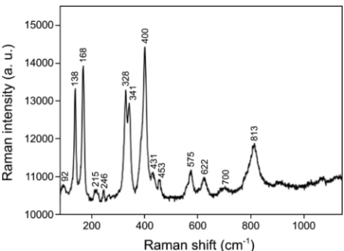
Raman spectrum of a thin film of NbO2 has been reported.28
We measured Raman spectrum of as-synthesized NbO2 NWs
with a home-built micro-Raman system using a 633 nm He-Ne laser as an excitation source. Figure 5 shows a typical Raman spectrum of NbO2 NWs ensemble, which is quite
similar to that of an NbO2 thin film except two peaks under
100 cm−1 and above 1,000 cm−1.
Figure 4. (a) Representative TEM image and SAED pattern of an individual NbO2 NW. The black arrow indicates the [001] growth direction. SAED pattern in inset is indexed for a tetragonal NbO2 NW down the [010] zone axis. (b) Representative high resolution TEM (HRTEM) image. The labeled distance of 0.2571 nm corres-ponds to the (202) plane. The inset shows the two-dimensional FFT from the HRTEM. (c) compositional line profile image scanned along the radial direction (red line) of a NbO2 NW.
842 Bull. Korean Chem. Soc. 2012, Vol. 33, No. 3 Sunghun Lee et al.
Conclusion
We have successfully synthesized single crystalline NbO2
NWs by chemical vapor transport method. Structural charac-terization via TEM analyses confirms the single crystalline nature and the elemental composition of NbO2 NWs. We
suggest that NbO2 NWs grow by self-seeded growth after
forming a thin film of NbO2. We also investigated the Raman
spectrum peaks of NbO2 NWs ensemble. The thin NbO2
NWs synthesized in this work could be used for the elec-trochemical sensors and fuel cells applications.
Acknowledgments. This research was supported by the NRL (2011-0020419).
References
1. Rao, C. N. R. Annu. Rev. Phys. Chem. 1989, 40, 291.
2. Poizot, P.; Grudeon, S.; Dupont, L.; Tarascon, J. M. Nature 2000, 407, 496.
3. Julien, C.; Haro-Poniatowski, E.; Camacho-López, M. A.; Escobar-Alarcón, L.; Jímenez-Jarquín, J. Mater. Sci. Eng. B 1999, 65, 170. 4. Ponzi, M.; Duschatzky, C.; Carrascull, A.; Ponzi, E. Appl. Catal.
A 1998, 169, 373.
5. Micocci, G.; Serra, A.; Tepore, A; Capone, S.; Rella, C. R.;
Siciliano, P. J. Vac. Sci. Technol. A 1997, 15, 34.
6. Kanan, S. M.; El-Kadri, O. M.; Abu-Yousef, I. A.; Kanan, M. C. Sensors 2009, 9, 8158.
7. Krusin-Elbaum, L.; Wittmer, M. J. Electrochem. Soc. 1988, 135, 2610.
8. Chen, Z.; Cummins, D.; Reinecke, B. N.; Clark, E.; Sunkara, M. K.; Jaramillo, T. F. Nano Lett. 2011, 11, 4168.
9. Lee, H. -W.; Muralidharan, P.; Ruffo, R.; Mari, C. M.; Cui, Y.; Kim, D. K. Nano Lett. 2010, 10, 3852.
10. Feng, X.; Shankar, K.; Varghese, O. K.; Paulose, M.; Latempa, T. J.; Grimes, C. A. Nano Lett. 2008, 8, 3781.
11. Okaz, A. M.; Keesom, P. H. Phys. Rev. B 1975, 12, 4917. 12. Friedrichs, O.; Sanchez-Lopez, J. C.; Lopez-Cartes, C.; Klassen,
T.; Bormann, R.; Fernandez, A. J. Phys. Chem. B 2006, 110, 7845. 13. Orel, B.; Macek, M.; Grdadolnik, J., Meden, A. J. Solid State
Electrochem. 1998, 2, 221.
14. Kurioka, N.; Watanabe, D.; Haneda, M.; Shimanouchi, T.; Mizushima, T.; Kakuta, N.; Ueno, A.; Hanaoka, T.; Sugi, Y. Catal. Today 2003, 16, 495.
15. Kimura, S. J. Solid State Chem. 1973, 6, 438.
16. Hulm, J. K.; Jones, C. K.; Hein, R. A.; Gibson, J. W. J. Low Temp. Phys. 1972, 7, 291.
17. Rao, C. N. R.; Wahnsiedler, W. E.; Honig, J. M. J. Solid State Chem. 1970, 2, 315.
18. Cho, N. -H.; Kang, H. B.; Kim, Y. H. Ferroelectrics 1994, 152, 43.
19. Natio, K.; Kamegashira, N.; Sasaki, N. J. Solid State Chem. 1980, 35, 305.
20. Helali, S.; Abdelghani, A.; Hafaiedh, I.; Martelet, C.; Prodromodis, M. I.; Albanis, T.; Jaffrezic-Renault, N. Mat. Sci. Eng. C 2008, 28, 826.
21. Sasaki, K.; Zhang, L.; Adzic, R. R. Phys. Chem. Chem. Phys. 2008, 10, 159.
22. Orilall, M. C.; Matsumoto, F.; Zhou, Q.; Sai, H.; Abru a, H. D.; DiSalvo, F. J.; Wiesner, U. J. Am. Chem. Soc. 2009, 131, 9389. 23. Mozeti , M.; Cvelbar, U.; Sunkara, M. K.; Vaddiraju, S. Adv.
Mater. 2005, 17, 2138.
24. Lin, Y.; Yang, Y.-J.; Hsu, C.-C. Thin Solid Films 2011, 519, 3043. 25. In, J.; Yoon, I.; Seo, K.; Park, J.; Choo, J.; Lee, Y.; Kim, B. Chem.
Eur. J. 2011, 17, 1304.
26. Yoon, H.; Seo, K.; Moon, H.; Varadwaj, K. S. K.; In, J.; Kim, B. J. Phys. Chem. C 2008, 112, 9181.
27. (a) Harjanto, S.; Shibayama, A.; Sato, K.; Suzuki, G.; Otomo, T.; Takasaki, Y.; Fujita, T. Resources Processing 2005, 52, 113. (b) Pershina, V.; Sepp, W. -D.; Bastug, T.; Fricke, B.; Ionova, G. V. J. Chem. Phys. 1992, 97, 1123.
28. Zhao, Ye.; Zhang, Z.; Lin, Y. J. Phys. D: Appl. Phys. 2004, 37, 3392.
n
ê cê
Figure 5. A typical Raman spectrum of NbO2 NWs ensemble at room temperature excited with 633 nm light.
![Figure 4. (a) Representative TEM image and SAED pattern of an individual NbO 2 NW. The black arrow indicates the [001] growth direction](https://thumb-ap.123doks.com/thumbv2/123dokinfo/5082435.74791/3.892.94.409.136.1024/figure-representative-image-pattern-individual-indicates-growth-direction.webp)