ICCAS2005 June 2-5, KINTEX, Gyeonggi-Do, Korea
1. INTRODUCTION
Analog multiplier are basic circuit building blocks for analog signal processing in instrumentation and communication systems such as a variable gain amplifier, automatic gain control amplifier, frequency doubler, phase locked loop, amplitude locked loop, small signal rectifier, etc. In the present, the most received attention analog multipliers are implemented in the form of integrated circuit [1]-[2]. The realization method of these approaches is based on the use of the translinear characteristic of transistors operating in saturation region. However, a specific circuit is required to perform a multiplication function. It is well know that an output stage of a general-purpose opamp is usually a class AB configuration. The operation of a class AB output stage is based on the translinear principle. Therefore, the opamp with a class AB output stage can be employed as a basic active element in the realization of an analog multiplier. The translinear characteristic of an opamp with class AB output stage is existed within the supply current of the opamp. The opamp supply current sensing technique [3]-[4] is employed to obtain the square of the sum and difference of two input signals. The multiplication is achieved by the quarter-square algebraic identity. The purpose of this article is to propose analog multiplier using operational amplifier. The realization method is based on the use of a translinear principle and quarter-square technique. The proposed circuit is required three general-purpose opamps together with resistors, which provides high performance, simple construction and low cost attraction.
2. CIRCUIT DESCRIPTION
2.1 Quarter-square technique
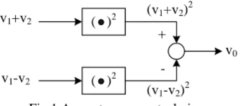
The proposed analog multiplier is based on the quarter-square technique as shown in Fig. 1. The sum and difference of the input v1 and v2 are provided for the squares.
The difference of squares at the output v0 is obtained to get
the multiplication function and can be written as
v0 = [(v1 + v2)2 – (v1 – v2)2] = 4v1v2 (1)
From Fig. 1, a square circuit is an important element in the quarter-square technique. Previously, many schemes to realize a square circuit can be found in the literature [5] – [10]. It is known that the class AB characteristic at the output stage of the opamp can be exploited to realize a squaring scheme [5].
( )2 ( )2 v1+v2 v1-v2 + -v0 (v1+v2)2 (v1-v2)2
Fig.1 A quarter-square technique
2.2 Characteristic of the class AB output stage
Fig. 2(a) shows a unity gain voltage controlled voltage source using an opamp. The class AB output stage of an opamp is shown in Fig 2(b) transistors in saturation region. From Fig. 2, the relation of the supply currents I1 and I2
depicted in Fig 2(a) are comprised of the quiescent bias current drawn by the opamp and the currents I01 and I02 or
I1 = IB +
+ I01 (2a)
I2 = IB- + I02 (2b)
Where IB+ and IB- are the bias currents drawn by the opamp.
In general, the magnitude of the bias current IB +
and IB
are quite variable from opamp to opamp.
iin I1 I2 vin
IS Io1 iin Io2 IS Q1 Q2 Q3 Q4 (a) (b)
Fig. 2 Principle of the Class AB output stage Assuming that all transistors in Fig. 2(b) is well matched, the current I01 and I02 in the Fig. 2(b) can be approximately given by [5] 2 } i ) i I 4 {( I in 2 / 1 2 in 2 S 01 − + = for | iin | ≤ 2IS (3a)
Analog multiplier using operational amplifier
Wandee Petchmaneelumka*, Kiettiwan Songsataya*, Vanchai Riewruja*, and Prasit Julsereewong**
* Department of Control Engineering, Faculty of Engineering, **Department of Instrumentation Engineering, Faculty of Engineering, King Mongkut’ s Institute of Technology Ladkrabang, Bangkok, Thailand
(Tel : +66-2-739-0757; E-mail: [email protected])
Abstract: In this article, presents an analog multiplier using a general-purpose operational amplifier (opamp). The realization
method is based on the quarter-square technique, which utilize the square-law characteristic of the class AB output stage of the opamp. The experimental results verifying the proposed multiplier performances are also included. The linearity error and the total harmonic distortion is about 0.8% and 1.6%, respectively.
Keywords: analog multiplier, operational amplifier, quarter-square technique
ICCAS2005 June 2-5, KINTEX, Gyeonggi-Do, Korea
2 } i ) i I 4 {( I in 2 / 1 2 in 2 S 02 + + = for | iin | ≤ 2IS (3b)
where IS is the class AB bias current. It should be noted that a
square signal is existed in the supply currents I1 and I2. 2.3 Squaring scheme
A simple squaring scheme is shown in Fig. 3 [5].
v
-R
cR
1R
S1R
f2R
x R2v
inv
ov
1v
2 A1R
S2R
f1I
1 I2 A2v
+I
Rs1I
Rs2 iinFig. 3 A simple squaring scheme
The opamp A1 and converting resistor Rx convert an input
signal voltage vin into a signal current iin = vin / Rx. For the
opamps A1 and A2 implemented in bipolar technology, the
currents I1 and I2 can be given by the use of Eq. (2) and (3) as
I1 = IB + + 2 } i ) i I 4 {( in 2 / 1 2 in 2 S+ − for | i in | ≤ 2IS (4a) I2 = IB- + 2 } i ) i I 4 {( S2+ in2 1/2+ in for | iin | ≤ 2IS (4b)
The currents I1 and I2 are, respectively, converted by the
sensing resistors R1 and R2 to the voltage v1 and v2. The
voltages v1 and v2 are transferred to the summing amplifier,
formed by the opamp A2 and resistors Rf1, Rf2, RS1 and RS2.
Assuming that I1 >> IRS1 and I2 >> IRS2, where IRS1 and IRS2
are the currents through the resistors RS1 and RS2, respectively.
If R1 = R2 = R, RS1 = RS2 = RS, Rf1 = Rf2 = Rf and v +
= -v- = v then the output voltage v0 can be expressed as
2 / 1 2 2 in S S f C f B S f 0 ) I 4 i 1 ( I R RR 2 v R R I R RR 2 v S + + − = (5)
The square-root term in the Eq. (5) can be expanded using the power series and then the Eq. (5) becomes
⎥ ⎥ ⎦ ⎤ ⎢ ⎢ ⎣ ⎡ + ⎟⎟ ⎠ ⎞ ⎜⎜ ⎝ ⎛ − ⎟⎟ ⎠ ⎞ ⎜⎜ ⎝ ⎛ + ⎟⎟ ⎠ ⎞ ⎜⎜ ⎝ ⎛ − + = ( ) v i i ... v 4 S in 2 S in S S f C f S B S f 0 I 2 8 1 I 2 2 1 R I RR 2 R R I I R RR 2 (6)
It should be noted that the first term in the right side of the Eq. (6) is the DC component and can be eliminated by setting
(Rf / RC)v = (2RRf / RS)(IB + IS). If the magnitude of the signal
current iin is chosen such that iin << 2IS, then the output
voltage v0 can be given as
2 in 1 2 X in S S f 2 in S f 0 K (v ) R v I R 4 RR ) i ( Is R 8 RR 2 v ⎟⎟ = ⎠ ⎞ ⎜⎜ ⎝ ⎛ = = (7a) S 2 X S f 1 I R R 4 RR K = (7b)
It is evident that the output voltage v0 is the square of the
input voltage vin with the scale factor K1.
2.4 Multiplier realization
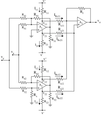
The proposed analog multiplier using opamp is shown in Fig. 4. The circuit consists of three general-purpose opamps A1, A2,
A3 and resistors. The opamps A1, A2 and resistors R31 = R32 =
R3 are connected as a voltage-to-current converter.
v -v -R11 Rs11 R21 vo v11 v21 Rs21 Rf I11 I21 A3 v+ IRs11 IRs21 A1 R12 Rs12 R22 vx v12 v22 Rs22 I12 I22 v+ IRs12 IRs22 A2 vy R31 R41 R51 R42 R52 R32 R61 R62 Rx
Fig. 4 Proposed analog multiplier
The resistors R11, R21, R12 and R22 are used to sense the supply
current and set R11 = R12= R1, R21 = R22 = R2, R1 = R2. In Fig.
4, the output voltage v01 and v02 from opamp A1 and A3, A2
and A3, respectively, can be expressed as
2 y x 1 2 X y x S S f 2 31 S f 01 K(v v ) R v v I R 4 RR ) i ( Is R 8 RR 2 v ⎟⎟ = + ⎠ ⎞ ⎜⎜ ⎝ ⎛ + = = (8a) 2 y x 1 2 X y x S S f 2 32 S f 02 K (v v ) R v v I R 4 RR ) i ( Is R 8 RR 2 v ⎟⎟ = − ⎠ ⎞ ⎜⎜ ⎝ ⎛ − = = (8b)
where vx and vy are the input signal voltages. The voltage v01
and v02 are transferred to the difference amplifier formed by
the opamp A3 and resistors RS11 = RS21 = RS12 = RS22 = RS and
ICCAS2005 June 2-5, KINTEX, Gyeonggi-Do, Korea
Rf1 = Rf2 = Rf. As a result, the output voltage v0 is given by
02 01
0 v v
v = − (9)
Substituting Eq. (8a) and (8b) into Eq. (9), then the output voltage v0 is given by y xv v K v0= 2 (10) 2 X S S f 2 R R I RR K = (11)
It can be seen that the general-purpose operational amplifier can be realized an analog multiplier using the proposed structure.
3. EXPERIMENTAL RESULT
The performance of the proposed multiplier depicted in Fig. 4 was shown experimentally. The opamp LM741 was chosen for demonstrating the performance of the proposed multiplier. The resistors used were in the form of 1% tolerance, where R1
= R2 = 2kΩ, R3= 10kΩ, R4 = R5 = R6 = RS = Rx = 100kΩ and
Rf = 200kΩ. The power supply voltages v +
= -v- were set to 6V.
Fig. 5 DC transfer characteristic
Fig. 6 Linearity error
The DC transfer characteristic is shown in Fig. 5. The dynamic range of the input voltage vx and vy of about ±1V is
observed. Fig 6 shows the measured linearity error for the input voltage varied from –1.25V to 1.25V. The worse-case linearity error is about 7.9mV or relative error of 0.8% in ±1V input dynamic range. The output response of the proposed multiplier is determined in two cases. For the first case, the signal voltage is applied to the input vx, while the input vy is
set to dc voltage. The second case is that the input vx and vy in
the first case are interchanged.
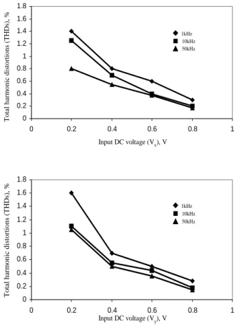
0 0.2 0.4 0.6 0.8 1 1.2 1.4 1.6 1.8 0 0.2 0.4 0.6 0.8 1 1kHz 10kHz 50kHz To tal har m oni c dis tor tio ns ( T H D s) , % Input DC voltage (Vx), V 0 0.2 0.4 0.6 0.8 1 1.2 1.4 1.6 1.8 0 0.2 0.4 0.6 0.8 1 1kHz 10kHz 50kHz Total ha rm on ic dis tor tions ( T H D s) , % Input DC voltage (Vy), V
Fig. 7 Total harmonic distortion
Fig. 8 Multiplying result of sinusoidal 100kHz amplitude 1Vp-p with triangle 1kHz amplitude 1Vp-p
ICCAS2005 June 2-5, KINTEX, Gyeonggi-Do, Korea
The total harmonic distortions (THDs) versus the input
voltage at 1kHz, 10kHz and 50kHz of the amplitude 1Vp-p are
shown in Fig. 7 for the both case. The maximum THD of about 1.6%, are observed. Fig. 8 shows the multiplying result of a 100kHz sinusoidal of amplitude 1Vp-p and a 1kHz
triangular wave of the amplitude 1Vp-p applied to the input vx
and vy, respectively. It should be noted that the scale factors of
the proposed multiplier using opamp is about 0.75. From the experimental results, it is clearly seen that the proposed multiplier exhibits an adequate basic performance for analog signal processing.
4.CONCLUSION
The analog multiplier based on a quarter-square technique using general-purpose opamp has been presented. The opamp supply-current sensing was used to provide a sum-square and difference-square function. The multiplication function was obtained by the result of the difference of sum-square and difference-square of the input signals. The performance of the proposed multiplier has been demonstrated by experimental implementation. The results indicate that the proposed multiplier provides high performance and offers the advantage of the simple circuit configuration and low cost required.
REFERENCES
[1] Muhammad Taher Abuelma’Atti; Sotian Mustafa Abed: A translinear circuit for sinusoidal frequency multiplication. Int. J. electronics 1999, vol.86, no. 1, 35-41.
[2] Bratt A.H.; King D.; Lysejko M.J.: Integrated analogue voltage multiplier combining MOS and bipolar transistors. Electron. Lett. 1991, vol. 27, no. 20, 1852-1854.
[3] Huijsing J. H.; Lucas P.; De Bruin B.: Monolithic analog multiplier-divider. IEEE J. Solid-State Circ. 1987, vol. 17, no. 1, 9-15.
[4] Pena-Finol J. S.; Connelly J. A.: A MOS four-quadrant analog multiplier using the quarter-square technique. IEEE J. Solid-State Circ. 1982, vol. 22, no. 6, 1064-1073.
[5] Surakampontorn W.: Sinusoidal frequency doublers using operational amplifiers. IEEE Trans. Inst. & Meas. 1988, vol. 37, no. 2, 259-262.
[6] Lidgey F.J.; Su W.J.: Improvements to opamp power-supply current sensing technique. Electron. Lett. 1994, vol. 30, no. 19, 1567-1568.
[7] Ashok S.: Integrable sinusoidal frequency doubler. IEEE J. Solid-State Circ. 1976, vol. 11, no. 2, 341-343. [8] Surakampontorn W.; Riewruja V.: Integrable CMOS
sinusoidal frequency doubler and full-wave rectifier. Int. J. electronics 1992, vol. 73, no. 3, 627-632.
[9] Surakampontorn W.; Anuntahirunrat K.; Riewruja V.: Sinusoidal frequency doubler and full-wave rectifier using translinear current conveyor. Electron. Lett. 1998, vol. 34, no. 22, 2077-2079.
[10] Anuntahirunrat K.; Tangsrirat W.; Riewruja V.; Surakampontorn W.: Sinusoidal frequency doubler and full-wave rectifier based on translinear current-controller current conveyors. Int. J. electronics 2004, vol. 91, no. 4, 227-239.