433 Journal of International Conference on Electrical Machines and Systems vol. 3, no. 4, pp. 433~445, 2014
Research on Discontinuous Pulse Width Modulation Algorithm for
Single-phase Voltage Source Rectifier
Xi-Jun Yang *, Hao Qu *, Hou-Jun Tang *, Chen Yao *,
Ning-Yun Zhang *, and Frede Blaabjerg **
Abstract -
Single phase voltage source converter (VSC) is an important power electronicconverter (PEC), including single-phase voltage source inverter (VSI), single-phase voltage source rectifier (VSR), single-phase active power filter (APF) and single-phase grid-connection inverter (GCI). As the fundamental part of large scale PECs, single-phase VSC has a wide range of applications. In the paper, as first, on the basis of the concept of the discontinuous pulse-width modulation (DPWM) for three-phase VSC, a new DPWM of single-phase VSR is presented by means of zero-sequence component injection. Then, the transformation from stationary frame (abc) to rotating frame (dq) is designed after reconstructing the other orthogonal current by means of one order all-pass filter. Finally, the presented DPWM based single-phase VSR is established analyzed and simulated by means of MATLAB/SIMULINK. In addition, the DPWMs presented by D. Grahame Holmes and Thomas Lipo are discussed and simulated in brief. Obviously, the presented DPWM can also be used for single-phase VSI, GCI and APF. The simulation results show the validation of the above modulation algorithm, and the DPWM based single-phase VSR has reduced power loss and increased efficiency.
Keywords:
Voltage source converter, Voltage source rectifier, Zero-sequence component,Discontinuous pulse width modulation, abc-dq coordinate transformation
1. Introduction
The traditional single-phase voltage source converter (VSC) is a full controlled bridge based two-level power electronic converter (PEC). According to different applications, It can work as different PECs, including single-phase voltage source inverter (VSI), single-phase active power filter (APF) and single-phase grid-connection inverter (GCI) and single-phase voltage source rectifier (VSR). When employed as single-phase AC-DC converter, it is an indispensable part in the traditional solid state converter (SST) [1-2].
When operating, it is inevitable that the power devices within the converter will produce power losses, which can reduce the overall efficiency and do harm to their service lives. Generally, the power losses include dynamic losses and static losses. The former includes turning-on loss and turning-off loss, which accounts for a large proportion and goes up with the increase of the switching frequency. The latter includes on-state loss and off-state loss, where on
state loss is related to on resistance and duty cycle, and off state loss can be neglected due to small percentage. Of course, the power losses are subject to the switching stress, including switching voltage and switching current.
The higher the entire power rating is, the more the overall power loss is. Many efforts are made to explore the heating mechanism, mathematical model, equivalent circuit and computation method [3-5].
In order to degrade the power losses, it is helpful to modify the modulation algorithm without the sacrifice of the waveform synthesis.
What’s exciting is that in the field of three-phase VSC, including active power filter, switching loss reduced PWM, i.e. discontinuous PWM has obtained much investigation with many outcomes [6-16]. The main principle is to inject an appropriate zero-sequence component into the original sinusoidal target function and gain a discontinuous or piecewise target function. There are durations where the maximum duty cycle is 1 or the minimum duty cycle 0. What is more is to make such durations fall into the neighborhood of peak current in order to decrease the resultant losses to a maximum extent.
In the paper, the above concept is introduced to single-phase VSC, dedicated to singe-single-phase VSR. And the DPWM
* Key Laboratory of Power Transmission and Conversion Control(Ministry of Education), Shanghai Jiao Tong University, China.([email protected])
** Dept. of Energy Technology, Alborg Universitet, Demark. Received 19 October 2014; Accepted 18 November 2014
of single-phase VSI/VSR by D. Grahame Holmes and Thomas Lipo is reviewed and simulated [17-18].
Dual closed-loop PI regulator can be applicable to three-phase VSR in the dq coordinate, where the d axis active power component and q axis passive power component can be controlled, respectively. Dual closed-loop PI regulator can also be applicable to single-phase VSR in the dq coordinate.
In order to obtain d and q axis component in dq coordinate, a general method is to reconstruct an orthogonal input current by phase shifting and 2x2 rotating transformation matrix [19-32]. A first-order all-pass filter is used which can effectively create the orthogonal current signal [33-34].
According to the above descriptions, a new DPWM based single-phase VSR is investigated in the paper, which is mainly arranged with the following structure:
Section 2 is provided with a simplified proof of solution multiplicity for single-phase VSR;
Section 3 is provided with the principle of abc-dq coordinate transformation and the presented DPWM;
Section 4 is provided with simulation analysis;
Section 5 is provided with principle of power loss calculation and calculation results.
2. Proof of Solution Multiplicity
2.1 The circuit topologies
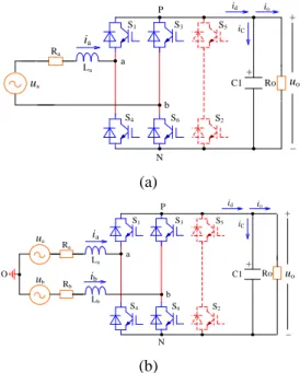
C1 -a b S1 S3 S4 S6 ia id La S5 S2 + ua Ra N P uo io iC Ro + (a) C1 a b S1 S3 S4 S6 ia La S5 S2 ua ub Lb Ra Rb ib N P O id io iC -+ uo + Ro (b)
Fig. 1. Power stage of single-phase VSR
The power stage of single-phase VSR is shown in Fig. 1(a), and another form is shown in Fig. 1(b), where reverse
conduction switches S1 and S4 constitute the first arm, and S3 and S6 constitute the second arm, and each reverse conduction switch consists of an IGBT and an anti-paralleled free-wheeling diode.
Single-phase VSR and single-phase VSI come from the same origin. The biggest difference between them resides in the different target functions in abc coordinate, or the different DQ components in DQ coordinate on the midpoint of the arms. The power stages of single-phase VSI, GCI and APF are shown in Fig. 2(a), 2(b) and 2(c).
-a b S1 S3 S4 S6 id E2 S5 S2 + N P La Lb Ra Rb ia ib C1 iC +
(a) Single-phase VSI
-a b S1 S3 S4 S6 E2 S5 S2 + N P Lf1 ia C1 iC + ui Lf2 Cf1 (b) Single-phase GCI C1 -a b S1 S3 S4 S6 ia id La S5 S2 + ua Ra N P uo io iC Ro + Non-linear load (c) Single-phase APF
Fig. 2. Power stages of single-phase VSI, GCI and APF
2.2 The solution multiplicity
Let k=a and b, and define double polarity switching function:
k
1, S1 or S3 is on and S4 or S6is off 0,S4 or S6 is on and S1 or S3 is off
S
= (1)
Considering the symmetry of the power system,
a b
0
e
e
(2)a b
=0
Assuming the instantaneous output DC voltage is uo with a limited voltage ripple, and the average output DC voltage is Uo, then according KVL and KCL, AC side voltage loop function and DC side current function are established as, respectively k k k 1 k o k k k a,b d 1 L R (S S ) dt 2 i e i u
(4) o o 1 a a b b L d u C S S dt R u i i (5)And Sk can be decomposed as
n k k k s n 1
2
S
d
( 1)
sin(nd
) cos(n
t)
n
(6)where
d
k is the mean value of switching functionS
kwithin the kth switching period, i.e. duty ratio.
For the sake of convenience and simplicity, the high frequency components within Fourier frequency spectrum are neglected, then equations (4) and (5) are rewritten as
k k k 1 k o k k k a,b d 1 L R (d d ) dt 3 i e i u
(7) o o 1 a a b b L d C d dt R u u i i u (8)Let duty ratio dk as unknown variable, the low frequency
mathematical model are rewritten as
AX
B
(9) T a b [d ,d ] X (10) a b 1 0 0 1 i i A (11) a a a a a o b b b b b o o o 1 L d ( R L ) / dt d ( R L ) / dt d C dt i e i u i e i u u u R B (12)Considering equations(2) and (3), the solution of equation(9) is a a a a a o o b o b b b b o d ( R L ) / dt d ( R L ) / dt i e i u u i u e i u X (13) where, k k k k k k d R L dt i
u e i stands for the voltage
function of the two arm midpoints, and
u
o additionalcomponents, which can be arbitrary components that conform to constraint conditions.
It is noted here that U0 refers in particular to zero-sequence component, which can make the new target functions symmetrical and consistent.
Define m as the modulation index on the two arm midpoints, where Ukm denotes the magnitude of voltages on the two arm midpoints
Rewrite equation (13) as ap 0 0 i B i B 0 bp 0 d d d msin(ω t+θ ) + = + msin(ω t+θ -α) d d d X (14)
where
ω
i represents mains voltage angularfrequency,
d
kp positive sequence component,d
o zerosequence components.
Due to
d
kp
[0,1]
, the of value ranged
o has toBecause the dkp has uniqueness of solution and d0 has multiplicity of solution under the given conditions, single-phase VSR has multiplicity of solution. From Equation (14), strictly speaking, d0 can be positive, negative or zero-sequence components. Normally, zero-zero-sequence component is chosen as d0.
2.3 Body
Full-length papers generally, for example, consist of introduction, nomenclature, if any, main parts of the body,
and conclusion.The font sizes of the section headings are
bold 11 pt and those of the subsection headings bold 10 pt, respectively.
3. Generation of DPWM
3.1 The dq coordinate transformation
In theory, well-designed PI regulator has better control results in dq coordinate than in abc coordinate, due to it can acquire infinite loop gain and the resultant zero steady state error at the fundamental frequency. Unlike three-phase VSR, single-phase VSR has to establish its own abc-dq coordinate transformation. An easy approach is to reconstruct the required orthogonal phase current with respect to the original phase current by directly shifting the initial phase of the original current by 1/4 mains period dynamically, or by first-order all-pass filter to create the required orthogonal signal. The first-order all-pass filter features unchanged magnitude of the filtered original signal while the initial phase is shifted. The transfer function of the first-order all-pass filter is given as
i f i ω -s G = ω +s (15)
As a result, the desired two components in stationary
coordinate are built up. Then conventional practice can be
used to complete the -DQ transformation. The-DQ
transformation matrix is cos( ) sin( ) T sin( ) cos( ) i i i i t t t t
(16)and the corresponding dq- transformation matrix is
1 cos( ) sin( ) T sin( ) cos( ) i i i i t t t t
(17) 3.2 The existing DPWMsSeveral PWM algorithms of single-phase VSI were introduced in Reference [15-16], inclusive of continuous SPWM and DPWM.
As for SVPWM, the two arms can only be modulated simultaneously. As for SPWM, the two arms can only be modulated individually.
The first DPWM can be represented as Fig.3 [16], where ua refers to the target function for the first arm, and ub refers to the target function for the other arm. The double polarity modulation is employed.
ua ub t 0 +1 -1 +1 -1 0 t
Fig. 3. Diagram of the first DPWM
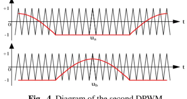
The second DPWM can be represented as Fig.4 [16], where ua refers to the target function for the first arm, and ub refers to the target function for the other arm. The double polarity modulation is employed.
ua ub t 0 +1 -1 +1 -1 0 t
Fig. 4. Diagram of the second DPWM
The two DPWM’s are characteristic of reduced average switching number, but the dynamic losses and static losses are not evenly distributed among the four IGBTs and four FWDs, respectively.
3.3 The presented DPWM
As for single-phase VSR, there are two basic device grouping methods. Reverse conduction switches S1 and S6,S3 and S4 are severally in a group, named grouping I, which merely can use double polarity continuous SPWM;
Reverse conduction switches S1 and S4,S3 and S6 are severally in a group, named grouping II, which can use double polarity continuous SPWM, the above said DPWMs,
and the other PWMs with zero-sequence component injection.
As for grouping II, the phase difference between the two fundamental target functions on the two midpoint of the
two arms can be (0, ).
Within any power electronic converters, it is inevitable for each power device to produce on loss, switching-off loss, on-state loss, and the omitted switching-off-state loss. A generalized loss expression of each power device was given in reference [35]. - -loss ds d s P g(U , I )f (18) where -ds
U indicates the average on-state voltage drop;
-d
I the average on-state current;
s
f
the average switching
frequency; Ploss is the monotonous increasing function of
-ds U and/or -d I
Equation (18) shows the importance to reduce s
f
and the necessity to move the non-switching zone to the maximum conduction current zone in order to reduce the switching loss to a great extent. Another critical point is to make all of the reverse conduction switches have the same power loss as the best possible.
SPWM features the inter-independent modulation among the arms, aiming at the target functions and phase voltage outputs on the midpoints of the arms, so by the insertion of zero-sequence components, it is likely to generate many different PWMs, such as the known saddle PWM, quasi-trapezoid PWM, DPWM, and even the equivalent SVPWM, etc.
SVPWM features the inter-dependent modulation among the arms, aiming at the circular voltage space vector trajectory synthesis and line voltage output between the midpoints of the arms, so by the arrangement of non-zero vectors and zero vectors, it is likely to generate many different PWMs, such as the known common-voltage reduction PWM, switching number reduction PWM, etc.
DPWM has already been investigated and applied in three-phase VSC by use of appropriate zero-sequence components [6-14]. Obviously, the generation of DPWM in three-phase VSC can be introduced to single-phase VSC.
Given three-phase symmetrical sinusoidal functions as the original target functions
a i b i c i m sin( ) m sin( - ) m sin( + ) u t u t u t
(19)where m is modulation index.
In Equation (21), the initial phase is zero. Actually, when the three-phase VSC works as three-phase VSR, the initial phase and m are determined by the working conditions.
a b c
max u u u
( , , )
andmin u u u
( , , )
a b c can be decomposed as DC component, zero-sequence components and even order harmonic components.In addition, the third, ninth, fifteenth order harmonic components and even DC component can also be taken into consideration. The linear combination of the above elements can be used as the final zero-sequence component.
Note that the even order harmonic components should be eliminated to make the resultant target function have the form of pure zero-sequence component.
An alternative zero-sequence component combination can be stated as [6-14] 0 a b c a b c - k m a x -( 1 - k m i n 2 k - 1 u u u u u u u ( , , ) ) ( , , ) ( ) (20)
where k is an arbitrary pulse train, K=1 or 0.
Then the new target functions of single-phase VSR are obtained as ' a a 0 ' b b 0 u u u u u u (21)
The addition of zero-sequence component changes the waveform of the original target function. Equation (21) contains the non-switching zone for a specific power device within a mains period, due to the occurrence of duty ratio with extreme value of 1 or 0.
The primary task is to make k vary with the phase displacement between mains voltage and mains current, and to arrange the non-switching zone fall into the neighborhood of peak mains current in order to minimize the switching losses.
4. Useful Hints
4.1 DPWM based three-phase VSR
In order to better understand the above said, some related waveforms of the DPWM based three-phase VSR are provided as background knowledge for single-phase VSR.
Fig.5 shows the waveforms of mains current, pulse train k, zero-sequence component u0, the fundamental function u0, and the final target function for the DPWM based three-phase VSR.
Fig.6 shows the waveforms of mains current and currents of IGBT S1, S2, S3 and S4 for the DPWM based three-phase VSR.
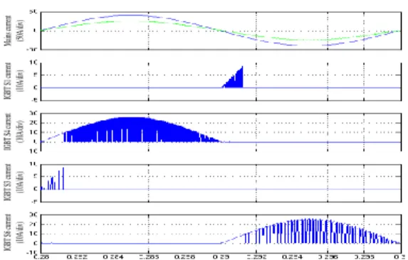
It can be seen from Fig.6 that it is easy to move the non-switching zone of power device IGBT to the peak mains current, meaning a reduced loss.
Time (5ms/div) IG BT S 6 c ur ren t (1 0A /di v) IG BT S 3 c ur ren t (1 0A /di v) IG BT S 4 c ur ren t (1 0A /di v) IG BT S 1 c ur ren t (1 0A /di v) M ain s c ur ren t (5 0A /di v)
Fig. 5. Waveforms of mains current, pulse train k,
zero-sequence component u0, the fundamental function u0, and the final target function, DPWM based three-phase VSR Time (5ms/div) IG BT S6 cu rre nt (10 A/ div ) IG BT S3 cu rre nt (10 A/ div ) IG BT S4 cu rre nt (10 A/ div ) IG BT S1 cu rre nt (10 A/ div ) M ain s c urr en t (50 A/ div )
Fig. 6. Waveforms of mains current and currents of IGBT
S1, S2, S3 and S4, DPWM based three-phase VSR
4.2 DPWM based single-phase VSR
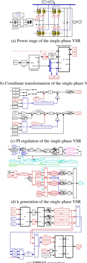
After combined with abc-dq coordinate transformation as well as well-configured PI regulation, a simulation platform of the presented DPWM based single-phase VSR is established by means of MATLAB/SIMULINK and simulated thoroughly.
Simulation conditions: singe-phase mains voltage is 120Vrms/50Hz, the desired DC voltage is 385V, the load
resistance is 74.11, the rated load power is 2.0kW, and
the boost inductance is 9.2mH, with DC resistance of 0.1.
Simulation platform of single-phase VSR is shown in Fig.7, where the power stage is in Fig.7 (a) , the coordinate transformation in Fig.7(b), the PI regulation in Fig.7(c), the k generation in Fig.7(d), the DPWM generation in Fig.7(e).
The frequency of k is three times of the mains frequency.
Because the specified IGBT is in off state within the 60
interval after the peak mains current, its initial phase is 30
leading to the mains current.
When the single-phase VSR works at PF=1, its initial
phase is 30 leading to the mains voltage/mains current.
The first-order all-pass filter can be used to gain the initial position of k. Measurement Discrete, Ts = 1e-006 s. powergui v + -Vdc4 A B C a b c A B C A B C N A B C Three-Phase Programmable Voltage Source RL g C E IGBT6 g C E IGBT4 g C E IGBT3 g C E IGBT1 [pulse] FWD6 FWD4 FWD3 FWD1 Convert DTC i +-CM8 i+ -CM7 i + -CM6 i+ -CM5 i +-CM4 i+ -CM3 i + -CM2 i + -CM10 i+ -CM1 C1 [Vdc] 1
(a) Power stage of the single-phase VSR
-u(1) wo4 xa xm sinth costh xd xq sinth1 costh1 ia fcn voltage clark/park/angle1 u(1)/311 com6 s-314 s+314 Transfer Fcn1 [sin] [cos] [Id] [Iq] [Vac] V (pu) Freq wt Sin_Cos 1-phase PLL
(b) Coordinate transformation of the single-phase VSR
i d* u(1)*2*pi *50*u(2)/u(3) wo2 u(1)*2*pi *50*u(2)/u(3) wo1 PI vol tage PI Control l er1 0
resi sti ve1 -12 i q* i nducti ve15 i q* capaci ti ve 10 i nductance4 1 i nductance3 1 i nductance2 5e-3 i nductance1 5e-3 i nductance PI PI 385 Vdc* Saturati on4 Saturati on2 Saturati on1 M ux M ux6 M ux M ux5 M S7 M S6 [uq] [ud] 1 1 1 [Iq] [Id] [Iq] [Id] [Vdc]
(c) PI regulation of the single-phase VSR
swi tch1 pul se f(u) i nducti ve l oad 50 i n freq. -pi *u(1)/0.01 capaci ti ve l oad pi /6 c6 9*pi /6 c5 11*pi /6 c4 5*pi /6 c3 7*pi /6 c2 pi /2 c1 ZOH 10 0.0001s+1 T rans Fcn1 T D1 Swi tch3 Swi tch2 In S S/H S&H M ux M ux6 M ux M ux5 M ux M ux4 M ux M ux3 M ux M ux21 M ux M ux2 M ux M ux1 T 1e-005 s M onostabl e M S4 NOT Log5 AND Log4 NOT Log3 NOT Log2 XOR Log1 up u lo y Interval T est Dynam i c2 up u lo y Interval T est Dynam i c1 up u lo y Interval T est Dynam i c 1 s Integrator u(1)+u(2) Fcn9 u(1)+u(3) Fcn8 u(1)-u(2) Fcn7 u(1)+u(2) Fcn6 u(1)+u(3) Fcn5 2*pi *u(1)*u(2) Fcn4 -(1*pi /6-u(1)) Fcn3 (u(1)-u(2))*pi /180 Fcn2 u(1)+u(2) Fcn11 u(1)+u(3) Fcn10 u(2)-u(1) Fcn1 Convert DT C2 Convert DT C1 0 Const.0~5 1 Const.0~3 Cl ock1 -30*pi /180 -pi /6 rad +30*pi /180 +pi /6 rad
(d) k generation of the single-phase VSR
InvPark sqrt(3/2)*u(1)/1.732 wo9 u(2)+u(4) wo8 u(1)+u(4) wo7 f(u) wo6 sqrt(3/2)*u(1)/1.732 wo5 sqrt(3/2)*u(1)/1.732 wo13 1/(20e3) t1 tcm1 tcm2 tcm3 pulse pul se1 ualf a ubata ua ub uc fcn a b c Vdc T tcm1 tcm2 tcm3 fcn ud uq costh sinth ualf a ubeta fcn z 1 z 1 z 1 T Del ay3 T Del ay2 T Del ay1 [pul se] PWM Mux Mux15 Mux Mux14 Mux Mux13 max Mi nMax1 mi n Mi nMax [ud] [Vdc] [cos] [si n] [uq] (e) DPWM generation
Fig. 7. Simulation platform of single-phase VSR, based on
DPWM (a) the power stage, (b) the coordinate transformation, (c) the PI regulation, the k generation, (e) the DPWM generation
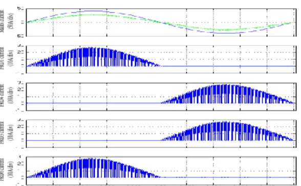
Fig.8 shows the waveforms of pulse train k, zero-sequence component u0, the fundamental function u0, and the final target function. Fig.9 shows the waveforms of mains current and currents of IGBT S1, S2, S3 and S4. Fig.10 shows the waveforms of mains current and currents of free-wheeling diode FRD1, FRD2, FRD3 and FRD4.
Time (5ms/div) tar ge t f un cti on fu nd am en tal fu nc tio n ze ro -se qu en ce co m po ne nt k M ain s c ur re nt (5 0A /d iv )
Fig. 8. Waveforms of pulse train k, zero-sequence
component u0, the fundamental function u0, and the final target function, based on the presented DPWM Time (5ms/div) IG BT S 6 c ur re nt (1 0A /d iv ) IG BT S 3 c ur re nt (1 0A /d iv ) IG BT S 4 c ur re nt (1 0A /d iv ) IG BT S 1 c ur re nt (1 0A /d iv ) M ain s c ur re nt (5 0A /d iv )
Fig. 9. Waveforms of mains current and currents of IGBT
S1, S2, S3, S4, based on DPWM, based on the presented DPWM Time (5ms/div) FR D 6 cu rre nt (1 0A /d iv ) FR D 3 cu rre nt (1 0A /d iv ) FR D 4 cu rre nt (1 0A /d iv ) FR D 1 cu rre nt (1 0A /d iv ) M ai ns c ur re nt (5 0A /d iv )
Fig. 10. Waveforms of mains current and currents of
free-wheeling diode FRD1, FRD2, FRD3 and FRD4, based on the presented DPWM
As for the presented DPWM, it is unlikely to make the non-switching zone distributed symmetrically on both side of peak mains current, or else, there can be more non-switching zones, and the current waveform will get more complicated.After more careful observation of the gained currents, the present DPWM has the following characteristics:
(1) The four IGBTs are constantly conducted within the non-switching zone, bringing about almost the identical switching losses, nevertheless the conduction losses are slightly different due to unsymmetrical current details;
(2) IGBT S1 and S4 constitute the first arm, and the
non-switching zone of S1 falls into the interval [270, 330],
and that of S4 [90, 150]. IGBT S3 and S6 constitute the
second arm, and the non-switching zone of S3 falls into the
interval [30, 90], and that of S6 [210, 270];
Accordingly, the non-switching zone of FRD1 [90, 150],
FRD4 [270, 330], FRD3 [210, 270], and FRD6 [30,
90];
(3) The current waveforms of FWD1 and S4, FWD4 and S1, FWD3 and S6, FWD6 and S3 are complementary, respectively, and the summations of them appear as half period sinusoidal waveforms.
4.3 SPWM single-phase VSR Time (5ms/div) IG BT S6 cu rre nt (10 A/ div ) IG BT S3 cu rre nt (10 A/ div ) IG BT S4 cu rre nt (10 A/ div ) IG BT S1 cu rre nt (10 A/ div ) M ain s c urr en t (50 A/ div )
Fig. 11. Waveforms of mains current and currents of IGBT
S1, S2, S3, S4, based on the SPWM Time (5ms/div) FR D6 cu rre nt (10 A/ div ) FR D3 cu rre nt (10 A/ div ) FR D4 cu rre nt (10 A/ div ) FR D1 cu rre nt (10 A/ div ) M ain s c urr en t (50 A/ div )
Fig. 12. Waveforms of mains current and currents of
free-wheeling diode FRD1, FRD2, FRD3 and FRD4, based on the SPWM
In order to make comparisons, the traditional continuous SPWM based single-phase VSR is simulated under the same conditions.
Fig.11 shows the waveforms of mains current and currents of IGBT S1, S2, S3 and S4.
Fig.12 shows the waveforms of mains current and currents of free-wheeling diode FRD1, FRD2, FRD3 and FRD4.
4.4 The exiting DPWMs based single-phase VSR
Time (5ms/div) IG BT S6 cu rre nt (1 0A /di v) IG BT S3 cu rre nt (1 0A /di v) IG BT S4 cu rre nt (1 0A /di v) IG BT S1 cu rre nt (1 0A /di v) M ain s c ur ren t (5 0A /di v)
Fig. 13. Waveforms of mains current and currents of IGBT
S1, S2, S3 and S4, based on the first existing DPWM Time (5ms/div) FR D6 cu rre nt (10 A/ div ) FR D3 cu rre nt (10 A/ div ) FR D4 cu rre nt (10 A/ div ) FR D1 cu rre nt (10 A/ div ) M ain s c urr en t (50 A/ div )
Fig. 14. Waveforms of mains current and currents of
free-wheeling diode FRD1, FRD2, FRD3 and FRD4, based on SPWM, based on the first existing DPWM Time (5ms/div) IG BT S 6 c ur re nt (1 0A /d iv ) IG BT S 3 c ur re nt (1 0A /d iv ) IG BT S 4 c ur re nt (1 0A /d iv ) IG BT S 1 c ur re nt (1 0A /d iv ) M ain s c ur re nt (5 0A /d iv )
Fig. 15. Waveforms of mains current and currents of IGBT
S1, S2, S3, S4, based on the second existing DPWM Time (5ms/div) FR D6 cu rre nt (10 A/ div ) FR D3 cu rre nt (10 A/ div ) FR D4 cu rre nt (10 A/ div ) FR D1 cu rre nt (10 A/ div ) Ma ins cu rre nt (50 A/ div )
Fig. 16. Waveforms of mains current and currents of
free-wheeling diode FRD1, FRD 2, FRD 3, FRD 4, based on SPWM, based on the second existing DPWM
Meanwhile, the former DPWMs based single-phase VSR is simulated under the same conditions, which were described by D. Grahame Holmes and Thomas Lipo. The first DPWM: Fig.13 shows the waveforms of mains current and currents of IGBT S1, S2, S3 and S4. Fig.14 shows the waveforms of mains current and currents of free-wheeling diode FRD1, FRD2, FRD3 and FRD4. The second DPWM: Fig.15 shows the waveforms of mains current and currents of IGBT S1, S2, S3 and S4. Fig.16 shows the waveforms of mains current and currents of free-wheeling diode FRD1, FRD2, FRD3 and FRD4.
According to simulation results of single-phase VSR using the above four PWMs, a conclusion can be drawn that different PWM leads to different current flowing through power devices including IGBTs and FWDs. Only the presented DPWM features the same switching number and symmetrical current distribution, perhaps it is a promising PWM for single-phase VSR.
In addition, like three-phase VSC, when working as the VSR or VSI, the switching waveforms of power devices with the same numbering for singe-phase VSR and single-phase VSI are quite different, due to the different power flow direction. Exactly, the current waveform via IGBT is the same as that of FWD with the same numbering.
5. Loss Calculation
Assuming the carrier frequency is all the same, nevertheless different modulation algorithm can lead to different static losses and dynamic losses, which can be formulated, calculated and compared.
5.1 The continuous SPWM
Take the device grouping I as instance, when the single-phase VSR reaches the steady state, with respect to the mains voltage, the target function can be written as
a m sin(ω t-θ )a i i u (22) ce π a im i (sat) i 0 m i i 1-1 I ) I ) 2π 2 sin(ω t U @[ sin(ω t]dω t u
(23)where the modulation ma and the initial phase angle
depend on the working conditions. Due to the symmetry of circuit and control, the four IGBTs have the same power losses, so do the four FWDs. The current waveforms through S1 and S6, S3 and S4 are identical, respectively. The current waveforms through S1 (S6) and S3 (S4) are different only in phase. Take power device S4 for instance, the average on-state loss can be derived as
where Im is the magnitude of mains sinusoidal current, Ud
is the instantaneous IGBT saturation voltage drop corresponding to the mains current.
The average switching loss is c 0.01f on off im i c n=1 E +E [@I sin ω ×n/f ]
( ) ( ) (24)where Eon and Eoff are the energy consumption during
every turning on and every turning off, respectively, fc is the
carrier frequency.
Take free-wheeling diode FWD1 for instance, the average on-state loss can be derived as following. Considering the target function of the first and second DPWM is piecewise continuous, and the calculation equation of the average on-state loss and the average switching loss are complicated, therefore the relevant equations are not provided any more.
ce π a im i (sat) i 0 m i i 1-1 I ) I ) 2π 2 sin(ω t U @[ sin(ω t]dω t u
(25)The average switching loss is c 0.01f err im o c n=1 E @[I sin ω ×n/f ]
( ) (26)where Eerr the energy consumption during every reverse
recovery.
5.2 The presented DPWM
The presented switching-number reduced DPWM can only employ the device grouping II. When the single-phase VSR reaches the steady state, with respect to the mains voltage, the target function can be written as
' a a i i o ' b b i i o m sin(ω t-θ ) m sin(ω t-α-θ ) u u u u (27)
The average on-state loss of power device S1 is
ce(sa ' 2π a im ) im i i π i U t 1+ 1 I ) @[I sin( d 2 sin(ω t ω )] π t 2 ω t u
(28)The average on-state loss of power device S4 is
c ' π a im e(sat) im 0 o o o 1-1 I d 2 sin(ω t) U @[I sin(ω ) 2π t] ω t u
(29)The average on-state loss of power device S3 is
c ' π b im e(sat) im 0 o o o 1+ 1 I d 2 sin(ω t) U @[I sin(ω ) 2π t] ω t u
(30)The average on-state loss of power device S6 is
c ' 2π b im o e(sa π t) im o o 1-1 d 2 I in(ω t) U @[I sin(ω t) ω t 2π ] u
(31)The average on-state loss of FRD1 is
d(sat ' π a im i ) im i i 0 U 1+ 1 I ) @[I sin( d 2 sin(ω t ω )] π t ω t 2 u
(32)The average on-state loss of FRD4 is
d(sa ' 2π a im im π i U t) i i 1-1 I ) @[I sin( d 2 sin(ω t ω )] π t ω t 2 u
(33)The average on-state loss of FRD3 is
d(sa ' 2π b im im π i U t) i i 1+ 1 I ) @[I sin( d 2 sin(ω t ω )] π t ω t 2 u
(34)The average on-state loss of FRD6 is
d(sa ' π im i t) im i i 0 U 1-1 I sin(ω t) @[I sinω t 2π 2 ( )]dω t b u
(35)The average switching loss of every IGBT is c c c 0.01f /6 on off im c n=1 0.01f on off im c n=1+0.01f /2 i i E +E @[I sin n/f ] + E +E @[I sinω n/f ] ω
( ) ( ) ( ) ( ) (36)The average switching loss of every FWD is c c c 0.01f /6 err im c n=1 0.01f err im c n=1+0. / i 01f 2 i E @[I sin n/f ] + E @[I sin n ω ω /f ]
( ) ( ) (37)5.3 Power Device loss analysis
Compared with the continuous SPWM, the presented DPWM has the following features:
(1) Power device IGBTs are in off state within interval
[30,90] or [90,150], and the switching number is
reduced by 1/3, leading a reduced switching loss, roughly by 40%;
(2) Power device FWDs are in on state within interval
[30,90] or [90,150], and the switching number is
reduced by 1/3, leading a reduced switching loss, roughly by 40%;
Apparently, the overall switching loss decreases, on the other hand, it needs to evaluate whether the overall conduction loss decreases or not. It is very difficult to exactly calculate the overall loss using the given equations, due to the nonlinear relation between the conduction voltage drop and conduction current.
For easy comparison, it is necessary to analyze the conduction losses in case of SPWM and the presented DPWM.
At first, in order to compare conduction loss, assuming the rising time and falling time are all 10ns, i.e. the switching speed of power device is high enough so that the switching losses can be ignored approximately.
It is also approximately assumed that the on resistance of
IGBT and FWD is 0.1, their forward voltage drop is
constant 1.5V. Then the single-phase VSR is simulated and made output the same power in the two cases. In which case the resultant mains current is lower, meaning the case features lower conduction loss, and vice versa.
As a consequence, the presented DPWM produces 18.46Arms mains current, the actual average output DC voltage is 385.0V, the ripple peak-peak value is 9V, and the overall efficiency is 90.285%. However, the SPWM produces 18.435Arms mains current, the actual average output DC voltage is 385.0V, the ripple peak-peak value is 9V, and the overall efficiency is 90.408%. The difference is +0.123%, indicating DPWM is slightly superior to SPWM in terms of conduction loss. It can be seen that the conduction losses are roughly the same.
Based on the above said about switching loss and conduction loss, a conclusion can be drawn that the overall loss is obviously reduced for the presented PWM when compared with the SPWM.
Then, in order to compare switching losses, assuming the
rising time is 1s, and falling time is 2s. Also
approximately assumed that the on resistance of IGBT and
FWD is 0.01, the forward voltage drop is constant 0.01V,
so that the conduction losses can be ignored approximately.
Consequently, the presented DPWM produces
17.50Arms mains current, the actual average output DC voltage is 385.0V, the ripple is 9V, and the overall efficiency is 95.25%. However the SPWM produces 17.62Arms mains current, the actual average output DC voltage is 385.0V, the ripple is 9V, and the overall efficiency is 94.54%. The difference is +0.70%, indicating DPWM is superior to SPWM in terms of switching loss. It can be seen that the switching losses are roughly different.
From the above simulation results, DPWM has the appreciably advantage over SPWM in terms of power device loss and conversion efficiency. Of course, the accurate data should come from reliable testing and precision measurement.
5.4 Calculation instances
It is difficult to precisely calculate the power loss according to the given data of power devices, because the practical working conditions are more different with the listed test conditions in given datasheet. Power devices from different manufactures have different performances and parameters in terms of design principle, manufacturing process and voltage/current rating.
According to the delivered power of 2.0kW, two kinds of IGBTs with anti-parallel FWDs built inside are chosen as candidate power device, shown in Fig.17 and Fig.18. The relevant curves and data come from their respective datasheet.
PM50CS1D060, produced by MITSUBISHI, which is
characteristic of 50A@25C, 600V, 3H bridge power
module, built-in free wheel diode, and the relation curves are shown is Fig.18.
(1) IPM PM25CS1D120:
PM 25CS1D120, produced by MITSUBISHI, which is
characteristic of 25A@25C, 1200V, one-bridge arm power
module, built-in free-wheeling diode, and the relation curves are shown is Fig.17.
(a) Uce(sat) vs Ic of IGBT (b) Ic vs VEC of FWD
(c) ON/OFF energy of IGBT (d) Recovery energy of FWD Fig. 17. Relation curves of PM25CS1D120
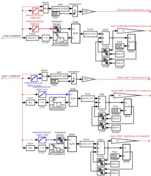
Within Simulink simulation environment, the loss calculation platform is established, shown in Fig. 19. At first, draw the above ten dotted characteristic curves
(@125C) into ten 1-D tables, and then look up IGBTs’
conduction voltage drop, switching on loss and switching off loss as well as FWDs’ forward voltage drops and reverse recovery losses according to these characteristic curves. Finally, calculate all the average losses within a mains period and fill the original data in Table 1. It can be seen from Table 1 that as for any power devices, in case of DPWM, the total losses within the single-phase VSR is much lower than those in case of SPWM. And the total switching loss in case of DPWM is much lower than those in case of SPWM. On the other hand, the total switching loss in case of DPWM is nearly the same as that in case of SPWM. The gained results are basically consistent with the simulated results in section 5.
(2) IPM PM50CS1D060
(a) Uce(sat) vs Ic of IGBT (b) Ic vs VEC of FWD
(c) ON/OFF energy of IGBT (d) Recovery energy of FWD Fig. 18. Relation curves of PM50CS1D060
6. Conclusion
Single-phase voltage source converter (VSC) has a long list of applications, and can be sorted into four types: single-phase VSI, single-phase VSR, single-phase APF, and single-phase GCI. They have the same basic working principle, except that the target functions in abc coordinate or the dq components in dq coordinate on the midpoints of the bridge arms are different, which is charge of the direction of power flow. In the paper, according to the discontinuous pulse-width modulation (DPWM) principle
of three-phase VSC, the DPWM of single-phase VSR is presented, analyzed and simulated by means of MATLAB/SIMULINK. The DPWM is realized by use of the injection of special zero-sequence component. Simultaneously, the continuous SPWM, the two existing DPWM presented by D. Grahame Holmes and Thomas Lipo are also introduced and simulated.
Each Di ode Conducti on Loss
Each IGBT Conducti on Loss
Each IGBT Swi tchi ng on Loss-Eon Each FWD Reverse Reconvery Loss
Each IGBT Swi tchi ng on Loss-Eoff
FWD CURRENT IGBT CURRENT abs(u(1)*u(2)) wo9 abs(u(1)*u(2)) wo5 T i VT D6 T i VT D5 T i VT D4 T i VT D3 T i VT D2 T i VT D1 T ransport Del ay3 T ransport Del ay2 In S S/H SH6 In S S/H SH5 In S S/H SH4 In S S/H SH3 In S S/H SH2 In S S/H SH1 PM25CS1D120 FWD Err PM25CS1D120 IGBT Ic-Vce PM25CS1D120 IGBT Eon PM25CS1D120 IGBT Eoff PM25CS1D120 FWD Vfd PG5 PG4 PG3 PG2 PG1 Mux Mux5 Mux Mux4 T 1e-006 s Monostable2 T 1e-006 s Monostable1 T 1e-006 s Monostable 1 s Integrator1 1 s Integrator 4*50 4*50 -K-u(1)-0.1 Fcn6 u(1)-0.117 Fcn5 f(u) Fcn4 u(1)-0.117 Fcn3 f(u) Fcn2 u(1)-0.117 Fcn1 50e-6 Const6 50e-6 Const5 50e-6 Const4 50e-6 Const3 50e-6 Const2 50e-6 Const1 > 0 CT Z2 > 0 CT Z1 > 0 CT Z Add2 Add1 Add
Fig. 19. Loss calculation platform (PM50CS1D060)
The latter can dramatically decrease the overall loss of the single-phase VSR, but the power losses are not evenly distributed among all the power devices. On the other hand, the presented DPWM can cause balanced power losses among the power devices. The presented DPWM has the following features: (1) Power device IGBTs are in off state
within interval [30, 90] or [90, 150]; (2) Power
device FWDs are in on state within interval [30,90] or
[90,150]; (3) The average switching number is reduced
by 1/3, leading a reduced switching loss, roughly by 40%; (4) The conduction losses is roughly unchanged, though in need of practical measurement. Unlike SPWM, the presented DPWM is kind of unsymmetrical modulation, leaving the following questions: (1) the practical value; (2) the effect on EMI distribution; (3) the distortion of mains current waveform synthesis due to the transition from switching zone to non-switching zone.
References
[1] Xu She, Alex Q. Huang, and Rolando Burgos. Review of Solid-State Transformer Technologies and Their Application in Power Distribution Systems. IEEE Journal of Emerging
and Selected Topics in Power Electronics, 1(3): 186-198, Sept. 2013.
[2] Jun Wang, Alex Q. Huang, Woongje Sung, Yu Liu, and B. JAYANT BAliga. Smart grid technologies: development of 15-kv SIC IGBTS and their impact on utility applications. IEEE industrial electronics magazine, pp: 16-23, June 2009. [3] Yan Xiong, Yanqun Shen, Jian Jiang, Xiangning He. Study
on loss calculation and loss model for IGBT. Power supply technologies and applications. 9(5): 55-60, 2006.05. (in Chinese)
[4] Mingyuan Zhang, Jiangqing Shen, Weichao Li, Shiguan geng, Zhengjun Tong. Calculation method of a fast power loss for IGBT modules. Marine Electric & Electronic Technology. 29(1): 33-36, 2009.01. (in Chinese)
[5] Qinlan Xie, Hong Chen. Loss calculating of IGBT’s in PWM inverters. Journal of South-central University for Nationality (Nat. Sci. Edition). 2003.03,22(1): 39-41. (in Chinese) [6] Dae-Woong Chung, Seung-Ki Sul. Minimum-loss strategy
for three-phase PWM rectifier. IEEE Transactions on Industrial Electronics. 46(3): 517–526, Jun. 1999.
[7] J. A. Houldsworth, D. A. Grant. The use of harmonic distortion to increase output voltage of a three-phase PWM inverter. IEEE Transactions on Industry. Application. 20(5): 1124–1228, Sept./Oct. 1984.
[8] Vladimir Blasko. Analysis of a Hybrid PWM Based on Modified Space-Vector and Triangle-Comparison Methods. IEEE Transactions on Industry Applications. 33(3): 756-764, May/Jun. 1997.
[9] Andrzej M. Trzynadlowski, Stanislaw Legowski. Comparison of the Effects of Continuous and Discontinuous PWM Schemes on Power Losses of Voltage-Sourced Inverters for Induction Motor Drives. IEEE Transactions on Power Electronics. 26(1): 182-191, Jan. 2011.
[10] Andrzej M. Trzynadlowski, Stanislaw Legowski. Minimum-loss vector PWM strategy for three-phase inverters. IEEE Transactions on Power Electronics. 9(1)1: 26-34, January 1994.
[11] Marcelo Cabral Cavalcanti, Edison Roberto Cabral da Silva, Antonio Marcus Nogueira Lima, Cursino Brandão Jacobina, Raimundo Nazareno Cunha Alves. Reducing losses in three-phase PWM pulsed DC-link voltage-type inverter systems. IEEE Transactions on Industry Applications, 38(4): 1114-1122, July/August 2000.
[12] Keliang Zhou and Danwei Wang. Relationship between space-vector modulation and three-phase carrier-based PWM a comprehensive analysis [three-phase inverters]. IEEE Transactions on Industrial Electronics, 49(1): 186-196, February 2002.
[13] Shaoliang An, Shaoliang An, Yanru Zhong, Mikihiko Matsui2. Research on a new and generalized method of discontinuous PWM strategies to minimize the switching loss. IEEE PES Asia (ISGT Asia), pp.1-6, 2012.
[14] Andrzej M. Trzynadlowski, R. Lynn Kirlin, Stanislaw F. Legowski. Space vector PWM technique with minimum switching losses and a variable pulse rate [for VSI] IEEE Transactions on Industrial Electronics. 44(2): 173-181, April 1997.
[15] Dae-Woong Chung, Seung-Ki Sul. Reduction of Switching Losses in Active Power Filters With a New Generalized Discontinuous-PWM Strategy. IEEE Transactions on Industrial Electronics. 46(3): 517-526, Jun. 1999.
[16] Lucian Asiminoaei, Pedro Rodriguez, Frede Blaabjerg, Mariusz Malinowski. Reduction of Switching Losses in Active Power Filters With a New Generalized
Discontinuous-PWM Strategy. IEEE Transactions on Industrial Electronics, Vol. 55, No. 1: 467-471, January 2008.
[17] A. M. Hava, R. J. Kerkman, and T. A. Lipo, A high performance generalized discontinuous PWM algorithm, IEEE Transactions Ind. Appl., 34(5): 1059–1071, Sep./Oct. 1998.
[18] D. Grahame Holmes, Thomas Lipo. Pulse width modulation for power converters: principle and practice[M]. John Wiley & Sons, 2003.10.3.
[19] Han Xiao, Yuannan Zeng, Xiongming Tang. Simulation of single-Phase PWM VSR with synchronous reference rotating frame. Telecom Power Technology. 2009.09,26(5): 43-46. (in Chinese)
[20] Wensheng Song, Xiaoyun Feng, Wangyu Xie. Space vector pulse width modulation and control technique for single-phase three level rectifier in d-q coordinate system. Electric Machines and Control. 2012.04,16(4): 56-63. (in Chinese) [21] Zhang R,Cardiml M,Szczesny P.A grid simulator with
control of single phase power conveners in d-q rotating frame[C]. IEEE 33rd Power Electronics Specialists Conference (PESC 2002), Vol. 3, pp. 1431-1436, 2002. [22] Salaet J,Busquets S,B0rdomu J.A new strategy for
decoupling direct and quadrature currents in a rotating frame current regulator[C].IEEE 37th Power Electronics Specialists Conference (PESC 2006), pp. 18-22, June 2006. [23] Salaet J I, A1epuz s, Gilaben A. Comparison between two
methods of DQ transformation for single phase converters control[C]. IEEE 35th Power Electronics Specialists Conference (PESC 2004), Vol. 1, pp.214-220, 2004. [24] Miranda U A, Aredes M, Rolim L G B. A DQ synchrounous
reference frame current control for single-phase converter[C].IEEE 36th Power Electronics Specialists Conference (PESC 2005), pp.1377-1831, 2005.
[25] Jirawut Benjanarasut, Bunlung Neammanee. The d-, q- axis control technique of single phase grid connected converter for wind turbines with MPPT and anti-islanding protection. Electrical power systems energy conversion. 2011 8th International Conference on the Electrical Engineering, Electronics, Computer, Telecommunications and Information Technology (ECTI) . pp. 649-652, 2011.
[26] S. Sakamoto, T. Izumi, T. Yokoyama, T. Haneyoshi. A new method for digital PLL control using estimated quadrature two phase frequency detection. Proc. PCC, pp. 671-676, Apr. 2002.
[27] M. Saitou, N. Matsui, T. Shimizu. A control strategy of single-phase active filter using a novel d-q transformation. [28] A. Roshan, R. Burgos, A.C. Baisden, F. Wang. A D-Q
frame controller for a full-bridge single phase inverter used in small distributed power generation systems. IEEE Twenty Second Annual Applied Power Electronics Conference. Vol.: l, pp.1-647, APEC 2007.
[29] A. R. Ram re -L pe , J. J. Lira-P rez, N. Visairo-Cruz, C.A. N e -Guti rre . Input-output linearization of a single-phase active multilevel rectifier in d-q synchronous reference frame. 12th International Power Electronics Congress (2010 CIEP), pp.15-20, 2010.
[30] Vinod Khadkikar, Ambrish Chandra. Control of single-phase UPQC in synchronous d-q reference frame. 2012 IEEE 15th International Conference on Harmonics and Quality of Power, pp.378-383, June 2012.
[31] Jirawut Benjanarasut, Bunlung Neammanee. The d-, q- axis control technique of single phase grid connected converter for wind turbines with MPPT and anti-islanding protection. The 8th Electrical Engineering/ Electronics, Computer,
Telecommunications and Information Technology, pp.649-652, May 2011.
[32] V. I Khadkikar, M. Singh, A. Chandra, B. Singh. Implementation of single-phase synchronous d-q reference frame controller for shunt active filter under distorted voltage condition. Power Electronics, Drives and Energy Systems, pp.1-6, Dec. 2010.
[33] S. Golestan, M. Monfared, J.M. Guerrero, M. Joorabian. A D-Q synchronous frame controller for single-phase inverters. 2011 2nd Power Electronics, Drive Systems and Technologies Conference, pp.317-323, Feb. 2011.
[34] B. H. Kwon, J. H. Choi, T. W. Kim. Improved single-phase line interactive UPS. IEEE Transactions Ind. Electron., 48(4): 804-811, Aug. 2001.
[35] B. K. Bose. Power Electronics and Variable Frequency Drives: Technology and Applications. Piscataway: IEEE Press, 1996.
Xijun Yang received the B.S. degree in
Electrical Drives from China University of Mining and Technology in Xuzhou, Jiangsu, P. R. China in 1992; the M.S. degree in Power Electronics from East China University of Metallurgy in Ma’anshan, An-hui, P. R. China in 1998; the Ph.D. degree in Control Engineering from Shanghai University in Shanghai, P. R. China in 2002; and gained certificate of post-doctoral from Shanghai Jiao Tong University in Shanghai, P. R. China in 2004; and worked with Shanghai Jiao Tong University in Shanghai, P. R. China from 2004, where he taught courses on Power Electronics and Electrical Drives as an Associate Professor at the Department of Electrical Engineering. From 1992 to 1995, he worked as an electrical engineer for Handan Institute of Coal Design and Research in Handan, Hebei, P.R. China, engaged in Electrical Engineering Design. Now, he is working as a guest associate professor in Department of Energy Technology, Aalborg University for one year till April, 2015.
Hao Qu received the B.S. degree in
Electrical engineering and automation from Shanghai Jiao Tong University in 2013. Now he is a postgraduate student in Shanghai Jiao Tong University, and the direction of research is on the power supply of plasma cutting machines.