P2-110 / D. Kim
• IMID 2009 DIGEST
Abstract
We investigated the influence of chemical compositions of gallium and indium cations on the performance of sol-gel derived amorphous gallium indium zinc oxide (a-GIZO) based thin-film transistors (TFTs). Systematical composition study allows us to understand the solution-processed a-GIZO TFTs. Understanding of the compositional influence can be utilized for tailoring the solution processed amorphous oxide TFTs for the specific applications.
1. Introduction
Amorphous oxide semiconductors have been attracting attention as channel layers of thin film transistors (TFTs) due to various their advantages, such as high mobility, device stability, and transparency.1-3 In addition, amorphous oxide semiconductors are preferred over polycrystalline counterparts from the viewpoints of low processing temperature and uniformity of device characteristics.1,4 Several amorphous oxide semiconductors, such as gallium indium zinc oxide (GIZO or IGZO)1,2,5, indium zinc oxide (IZO)6,7, zinc tin oxide (ZTO)8, and indium tin oxide (ITO)9, have been reported as a channel material in TFTs to date. These amorphous oxide semiconductors are mulicomponent materials and the electrical properties can be easily tuned for the specific functions by varying the compositions. In this regard, the understanding of compositional influence on the device performance is crucial to develop the multication-based oxide TFTs.
Amorphous oxide semiconductors have generally been fabricated by vacuum deposition methods such as chemical vapor deposition, radio frequency (rf) magnetron sputtering, and pulsed laser
deposition.3,5,6,10 However, the high manufacturing cost of vacuum processes poses an obstacle for low-cost large-area electronics. By contrast, solution-based printing method can offer many advantages such as simplicity, low cost, and high throughput that enable the direct fabrication of high-performance and low-cost electronics. For the formation of the complex oxide semiconductor from solution process, various precursor materials such as sol-gel solution and metal salts solution have been researched.11-13 Among them, the sol-gel solutions receive significant attentions because of accurate controllability in the composition and easy adaptability to various printing methods.
In this article, we fabricated the solution processed TFTs based on the sol-gel derived multicomponent GIZO active layer and investigated the influence of the relative compositions of Ga, In, and Zn cations on the device performance. The a-GIZO is known as the most promising candidate for TFTs.1,2,5 However, the detailed compositional study of the solution-processed a-GIZO has not been reported so far. We analyzed the influence of each metal cation on the device performance and generated a compositional ternary diagram in term of the device parameters.
2. Experimental
The sol-gel solution for the GIZO semiconducting film was prepared by dissolving zinc acetate dihydrate (Zn(CH3COO)2·2H2O), indium nitrate hydrate (In(NO3)3·H2O), and gallium nitrate hydrate (Ga(NO3)3·H2O) in 2-methoxyethanol. The total concentration of metal precursors was 0.3 M and the molar ratio of Ga, In, and Zn were varied from 0 - 0.2, 0.2 - 0.7 and 0.2 - 0.8, respectively (i.e., the molar ratio of Ga was varied from 0 to 0.2 for each fixed In:Zn molar ratio of 1:1, 2:1, 4:1, and 1:4). Ethanolamine was used as a stabilizing agent to improve the solubility of the precursor salts.
Influence of Compositions on Sol-Gel Derived Amorphous
In-Ga-Zn Oxide Semiconductor Transistors
Dongjo Kim, Chang Young Koo,
Keunkyu Song, Youngmin Jeong, and
Jooho Moon
Dept. of Materials Science and Engineering, Yonsei University, Seoul 120-749, Korea Tel.:82-2-2123-2855, E-mail: [email protected]
P2-110 / D. Kim IMID 2009 DIGEST • Glass 200nm-thick SiO2 Bottom-contact D G S GIZO
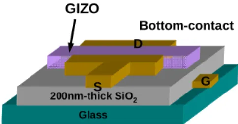
Fig. 1. Schematic picture of the fabricated TFT based on the a-GIZO semiconductor spin-coated on the SiO2/ITO/glass substrate.
We fabricated transistors in the bottom-contact and bottom-gate device configurations by spin-coating the GIZO sol-gel solutions on the ITO gate/source/drain electrodes with 300-nm thick SiO2. The width and length of the channel were 100 and 10 µm, respectively. The substrate was cleaned by isopropyl alcohol and UV-cleaner prior to deposition. The resulting films were dried at 200 oC for 90 s to evaporate the solvent and annealed at 400 oC for 30 min. The spin-coated films after annealing had a thickness of ~ 25 nm. Post-annealing step was then performed at 250 oC in vaccum atmosphere to improve the electrical performance of the TFTs. The schematics and microscopic image of the fabricated device were shown in Fig. 1.
20 30 40 50 In te n s it y (a rb . uni ts ) 2 theta (o) 200 oC 300 oC 400 oC 500 oC 600 oC
Fig. 2. X-ray diffraction patterns of sol-gel derived a-GIZO films annealed at 200 - 600 oC.
3. Results and discussion
We investigated the crystallinity of the sol-gel derived GIZO semiconducting layer. X-ray diffraction patterns revealed that the solution processed GIZO films have amorphous phase regardless of the chemical compositions and the amorphous structure maintained up to the annealing at 600 oC (Fig. 2). A broad peak from the a-GIZO layer was only seen at around 2θ=34o. No sharp peak features corresponding to the crystalline phase, i.e., GaInZnO4, Ga2O3, In2O3, and/or ZnO were observed.
In order to investigate the chemical compositions on the device performance of the a-GIZO TFTs, we fabricated the devices by varying ternary compositions of Ga, In, and Zn. All electrical measurements were carried out in air and in darkness using an Agilent 4155C semiconductor parameter analyzer. The saturation mobility (µsat) and threshold voltage (Vth) were estimated from a plot (ID)0.5 vs. VG in the saturation region as follows:
(1)
where ID is the drain current density, W and L are the channel width and length, Ci is the insulator capacitance, and VG and Vth are the gate and threshold voltage, respectively.
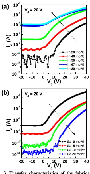
Fig. 3 shows the transfer characteristics for the fabricated TFTs as a function of chemical compositions. All the TFTs with different chemical compositions operated as a n-channel, enhancement-mode devices. With increasing the amount of In precursor, the on-current and off-current increased and the saturation mobility also increased from 0.003 to 0.05 cm2V-1s-1 (Fig. 3a). The threshold voltage was also shifted to negative voltage from 19.0 to 0.8 V and the increased off-current scarifies the on/off ratio. The determined ranges of on-current and off-current were about 10-7 - 10-5 A and 10-11 - 10-7 A, respectively. Correspondingly the on/off current ratio decreased from 3 × 10⁴ to 5 × 101. However, the influence of Ga in the a-GIZO system exhibited reverse tendency. The Ga addition decreased both the on-current and off-current, and reduced the field effect mobility from 0.03 to 0.003 cm2V-1s-1, and the threshold voltage shifted to positive voltage from 8.5 to 22.9 V (Fig. 3b). The on/off current ratio was slightly increased from 103 to 104 by the addition of Ga. The on-current and off-current were varied from 10-5 and 10-8 A to 10-7 and 10-12 A. 2
)
(
2
1
T G i eff DV
V
L
W
C
I
=
µ
−
P2-110 / D. Kim • IMID 2009 DIGEST -20 -10 0 10 20 30 40 10-12 10-11 10-10 10-9 10-8 10-7 10-6 10-5 In 20 mol% In 40 mol% In 50 mol% In 67 mol% In 80 mol% Vd = 20 V
I
d(A)
V
g(V)
-20 -10 0 10 20 30 40 10-11 10-10 10-9 10-8 10-7 10-6 Ga 0 mol% Ga 5 mol% Ga 10 mol% Ga 20 mol% Vd = 20 VI
d(A)
V
g(V)
(a)
(b)
Fig. 3. Transfer characteristics of the fabricated TFTs based on the sol-gel derived a-GIZO semiconductor as a function of precursor compositions: (a) the influence of indium without the addition of gallium; (b) the influence of gallium when In : Zn = 1 : 1.
The conduction band minimum (CBM) in the amorphous oxide semiconducting materials is primarily composed of unoccupied s-orbitals of a metal cation. By introducing the heavy post-transition cation with an electron configuration (n-1)d10
ns0
(where principal quantum number (n) ≥ 5), the spatial spread of this s-orbital is so large that direct overlap between the s-orbitals of neighboring cations is possible.1,2,14,15 This suggests that the incorporation of ns orbitals with larger principal quantum number is favorable for forming a conduction band minimum with a broader width, which allows for high electron mobility. The In3+ is heavy post-transition metal cation with a large principal quantum number (n=5) with
electronic configuration of [Kr](4d)10
(5s)0, whereas
Zn2+ has electronic configuration of [Ar](3d)10
(4s)0.
The addition of In3+ whose s orbital is larger than that of Zn2+, makes the oxide films more conductive due to the enhanced mobility as the extensive overlapping of neighboring s-orbitals originating from the added In3+ cations. This explains that the sol-gel derived a-GIZO TFTs exhibited the increases in both the on-current level and the field effect mobility with increasing In concentration (Fig. 3a).
In the case of Ga, on the other hand, the Ga ion can form stronger chemical bonds with oxygen that Zn and In ions, because Ga ion has high ionic potential of +3 valence and small ionic radius. This nature of Ga ion results in suppressing carrier generation via reducing the oxygen vacancy formation.14 Fig. 3b show that the Ga addition caused the decreases in the on-current, off-current, and field effect mobility, due to the reduced carrier concentrations. The decreased carrier can shift the threshold voltage, which is controlled by carrier concentration (i.e. donor concentration) in the channel, toward a positive voltage.7,16 Although Ga contents reduce the on-current and mobility, Ga plays an effective role in suppressing the formation of oxygen vacancies, reducing off-current with the increased on/off current ratio, which is critical in the practical application.
4. Summary
In summary, we fabricated the solution-processed oxide TFTs based on the multi-cation a-GIZO and investigated the influence of chemical compositions of gallium and indium cations on the device performance. Compositional influences of the sol-gel derived a-GIZO TFTs are similar with the results reported in the vacuum deposited counterparts. This information serves as a guideline to tune the chemical compositions in the sol-gel derived amorphous semiconducting layer for the specific applications.
Acknowledgement
This research was supported by Basic Science Research Program through the National Research Foundation of Korea (NRF) funded by the Ministry of Education, Science and Technology (Nos. R0A-2005-000-10011-0). It was also partially supported by the Second Stage of the Brain Korea 21 Project.
P2-110 / D. Kim
IMID 2009 DIGEST •
5. References
1. K. Nomura, H. Ohta, A. Takagi, T. Kamiya, M. Hirano, and H. Hosono, Nature (London), 432, p.488 (2004).
2. K. Nomura, A. Takagi, T. Kamity, H. Ogta, M. Hirano, and H. Hosono, Jpn. J. Appl. Phys., 45, p.4303 (2006).
3. H. Q. Chiang, J. F. Wager, R. L. Hoffman, J. Jeong, and D. A. Keszler, Appl. Phys. Lett., 86, p.013503 (2005).
4. R. Martins, P. Barquinha, L. Pereira, I. Ferreira, and E. Fortunato, Appl. Phys. A-Mater. Sci. Process., 89, p.37 (2007).
5. H. Yabuta, M. Sano, K. Abe, T. Aiba, T. Den, H. Kumomi, K. Nomura, T. Kamiya, and H. Hosono,
Appl. Phys. Lett., 89, p.112123 (2006).
6. N. L. Dehuff, E. S. Kettenring, D. Hong, H. Q. Chiang, J. F. Wager, R. L. Hoffman, C. H. Park, and D. A. Keszler, J. Appl. Phys., 97, p.064505 (2005).
7. P. Barquinha, A. Pimentel, A. Marques, L. Pereira, R. Martins, and E. Fortunato, J. Non-Cryst. Solids,
352, p.1749 (2006).
8. R. L. Hoffman, Solid-State Electron., 50, p.784 (2006).
9. T. Miyasako, M. Senoo, and E. Tokumitsu, Appl.
Phys. Lett., 86, p.162902 (2005).
10. M. D. Barankin, E. Gonzalez II, A. M. Ladwig, and R. F. Hicks, Sol. Energy Mater. Sol. Cells, 91, p.924 (2007).
11. G. H. Kim, H. S. Shin, B. D. Ahn, K. H. Kim, W. J. Park, and H. J. Kim, J. Electrochem. Soc., 156, p.H7 (2009).
12. C. Y. Koo, D. Kim, S. Jeong, J. Moon, C. Park, M. Jeon, W.-C. Sin, J. Jung, H.-J. Woo, S.-H. Kim, and J. Ha, J. Korean Phys. Soc., 53, p.218 (2008). 13. D. H. Lee, Y. J. Chang, G. S. Herman, and C. H.
Chang, Adv. Mater., 19, p.843 (2007).
14. H. Hosono, J. Non-Cryst. Solids, 352, p.851 (2006).
15. K. Nomura, T. Kamiya, H. Ohta, T. Uruga, M. Hirano, and H. Hosono, Phys. Rev. B, 54, p.11169 (1996).
16. T. Iwasaki, N. Itagaki, T. Den, H. Kumomi, K. Nomura, T. Kamiya, and H. Hosono, Appl. Phys.