이용자는 아래의 조건을 따르는 경우에 한하여 자유롭게 l 이 저작물을 복제, 배포, 전송, 전시, 공연 및 방송할 수 있습니다. 다음과 같은 조건을 따라야 합니다: l 귀하는, 이 저작물의 재이용이나 배포의 경우, 이 저작물에 적용된 이용허락조건 을 명확하게 나타내어야 합니다. l 저작권자로부터 별도의 허가를 받으면 이러한 조건들은 적용되지 않습니다. 저작권법에 따른 이용자의 권리는 위의 내용에 의하여 영향을 받지 않습니다. 이것은 이용허락규약(Legal Code)을 이해하기 쉽게 요약한 것입니다. Disclaimer 저작자표시. 귀하는 원저작자를 표시하여야 합니다. 비영리. 귀하는 이 저작물을 영리 목적으로 이용할 수 없습니다. 변경금지. 귀하는 이 저작물을 개작, 변형 또는 가공할 수 없습니다.
A THESIS
FOR THE DEGREE OF DOCTOR OF PHILOSOPHY
All-Printed Antennas Based on Transparent
Substrates for RF Electronic Devices
Arshad Hassan
Department of Ocean System Engineering
GRADUATE SCHOOL
JEJU NATIONAL UNIVERSITY
December, 2017
ii
Substrates for RF Electronic Devices
Arshad Hassan
(Supervised by Professor Jinho Bae)
A thesis submitted in partial fulfillment of the requirement for the degree of Doctor of Philosophy
2017. 12
The thesis has been examined and approved.
Thesis director, Dong-Guk Paeng, Professor, Department of Ocean System Engineering
Jinho Bae, Professor, Department of Ocean System Engineering
Yang-Hoi Doh, Professor, Department of Electronic Engineering
Yoon Hyeok Bae, Professor, Department of Ocean System Engineering
Woo Young Kim, Professor, Department of Electronic Engineering
Date
Department of Ocean System Engineering GRADUATE SCHOOL
JEJU NATIONAL UNIVERSITY REPUBLIC OF KOREA
iii
To
iv
Knowledge exists potentially in the human soul like the seed in the soil; by learning the potential becomes actual.
v
Acknowledgements
In the name of ALLAH, the Most Gracious, the Most Merciful. I would like to express my humble gratitude to Almighty ALLAH. HIS help and support is always with me and without HIS help i would not able to complete this thesis. HE bestowed me courage, patience and skills to complete the doctoral studies with ease and gratification. I would like to praise Almighty ALLAH as HE blessed me with humble Father and loving Mother. It’s truly a blessing having them in my life. Almighty ALLAH bless you both for being such loving parents. I am grateful to them for their eternal love, prayers, sacrifice and every kind of support throughout my life. Especially, i am indebted to my mother who has been extremely understanding, supportive and source of inspiration.
I learnt a lot during my stay in Ocean Information System Engineering (OISE) lab because the day i joined the lab, i was just familiar with research work but now, i can exercise my potential with full confidence in research for the welfare of human beings. This is all about guidance and schooling of my supervisor Prof. Jinho Bae. So, i would like to pay my thanks and best regards to Prof. Jinho Bae who put his energy and efforts to polish my research skills with innovative thoughts and ideas. I am thankful because his advice, support, trust, motivation and encouragement from the start to the end of my Ph.D. and also he played a vital role in the completion of this thesis work. I would also like to say thank to Prof. Jinho Bae gave me confidence and provided me shelter against all kind of crisis from morally depraved conditions to financial problems during my Ph.D. studies. I am also thankful to Prof. Chong Hyun Lee who gave valuable research guidance, ideas, pleasant environment and full access to his prestige laboratory to pursue the fruitful end of my research work.
I would like to pay my gratitude to my friend Dr. Shawkat Ali who introduced me to my supervisor Prof. Jinho Bae for postgraduate studies at OSE Lab, Jeju National University. I am grateful to Dr. Qasim Zeeshan Ahmed my advisor during master’s studies at National University of Computer and Emerging Sciences (FAST), Islamabad, Pakistan who encourage me to pursue my higher studies.
vi
prayers. I would like to extend my gratitude to my wife for taking caring of our blessed and lovely Son (Adil Khanzada). I feel sorry for my son who was neglected during my Ph.D. studies. I hope, i would make up for the time he spent without me in future. All of my family has always been a source of aspiration and admiration throughout my life either in my professional career or student life. Almighty Allah bestowed me such a noble and dominating figures in my life, without whom I could not have predicted myself to accomplish this task.
I really enjoyed the company of my colleagues at OISE lab and friends in Jeju National University. They provided such a lovely, pleasant and homely environment during my stay at Jeju National University. Few of the names are coming in my mind including Dr. Shawkat Ali, Gul Hassan, Irshad Ali, Umair, Waseem Abbas, Fasihullah, Asim Raza, Mamoon, Israr Ahmed, Dr. Shahid, Dr. Afaq, Kyani shab, Dr. Kamran Ali, Dr. Rasheed, Abdul Wahid, Dr. Jael Lee, Dr. Juhoo Kim, Kibae, Jhunhwa, Yuan Choi, Hansoo Kim, Mansoo, Younsang, Adeel, Muqeet, Fayaz, Jahanzeb, Mutee, Tahir, Imran, Dr. Zahid, Zubair and Dr. Farrukh. I would also like to thank my colleagues at NUCES-FAST Islamabad for their encouragement to pursue my Ph.D. studies which are: Dr. Waseem Ikram, Dr. Mukhtarullah, Dr. Ataul Aziz, Dr. Saeed, Aamir Munir, Rashid Karim, Ibrar Khan, Shibli Nisar, Waqas bin Abbas, Shehzad Ahmed and Niaz Ahmed.
In the end, I would like to acknowledge and promise myself to acquire wisdom with the help and blessing of Almighty ALLAH.
Arshad Hassan
vii
Abbreviations and Notations
EHD Electrohydrodynamic
2G Second Generation Cell-Phone Technology
3G Third Generation Cell-Phone Technology
LTE Long Term Evolution
FESEM Field Emission Scanning Electron Microscope
RF Radio Frequency 2D 3D DMP Two Dimensional Three Dimensional Dimatix Material Printer
HFSS High Frequency Structure Simulator
ITO Indium Tin Oxide
PET Polyethylene Terephthalate
OTFTs Organic Thin Film Transistors
SNP Silver Nano Particles
PDMS Polydimethylsiloxane
LEDs Light Emitting Diodes
OLEDs Organic Light Emitting Diodes
R2R Roll to Roll
DoD Demand on Drop
RFID GPS
Radio Frequency Identifications Global Positioning System
NFC Near Field Communications
UV Ultra Violet
CAD Computer Aided Design
VNA Vector Network Analyzer
CPW Coplanar Waveguide
DDM Dimatix Drop Manager
AUT Antenna Under Test
SMA Sub Miniature Version A
NI National Instruments
ISM Industrial, Scientific and Medical band
viii DC PSI Wi-Fi SOL HP FR-4 dBi Direct Current
Phase Shifting Interferometry Wireless Fidelity
Short-Open-Load Hewlett Packard Flame Retardant 4
Decibels referenced to Isotropic gain 𝑆11 Reflection Coefficient
𝜀𝑟𝑒𝑓𝑓 Effective Dielectric Constant
C Capacitance εr Dielectric Constant 𝑓𝑟 Resonance Frequency 𝑐0 Speed of Light L Inductance R Resistance 𝑍0 Characteristic Impedance 𝜆 Wavelength 𝑖 Electric Current 𝑞 Electric Charge 𝑣 Voltage 𝐿𝑏 𝐶𝑏 Bent Inductance Bent Capacitance
ix
List of Figures
Figure 1.1. Printed flexible antennas [5], [6]. ... 2
Figure 1.2. Various printing techniques based on solution-processed manufacturing [2]Error! Reference source not found.. ... 4
Figure 1.3. (a) Digital photograph of DMP-3000 inkjet material printer. (b) Schematic diagram of the DMP-3000 along main components [9]. ... 5
Figure 2.1. (a) Antenna design. (b) The equivalent electrical circuit of antenna. ... 10
Figure 2.2. (a) Equivalent T-network. (b) Lumped model of right angle bend. ... 13
Figure 2.3. The overall lumped circuit of antenna. ... 14
Figure 2.4. (a) Straight Geometry (b) Meander type bending geometry. ... 15
Figure 2.5. Reflection Coefficient of straight and meander type shapes ... 15
Figure 2.6. Right angle turn position variation along horizontal axis. ... 16
Figure 2.7. Reflection coefficients at different value of S. ... 17
Figure 2.8. Vertical length variation of the antenna with fixed total antenna length. 18 Figure 2.9. Reflection coefficient against vertical length variations. ... 19
Figure 2.10. Direct printing of the antenna on PET substrate using Dimatix Inkjet Material Printer. ... 20
Figure 2.11. Proposed fabricated printed antenna on a PET substrate (b) Transparent and flexible PET (with 0.04mm thick) based printed antenna mounted on Telos-B (inset). ... 21
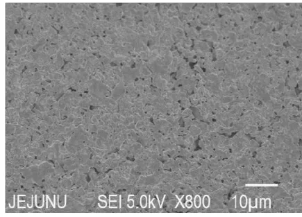
Figure 2.12. SEM Image of sliver nanoparticle ink layer after being cured at 50° for 2 h. ... 21
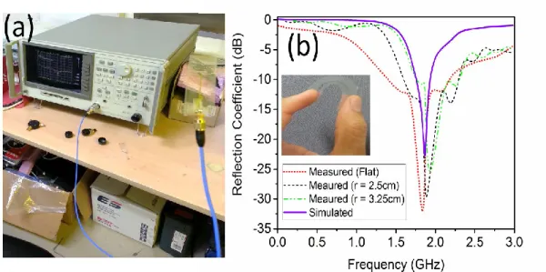
Figure 2.13. (a) Measured Reflection coefficient using HP vector network analyzer. (b) Measured (over different bending radii) and simulated reflection coefficient for the proposed printed antenna. ... 22
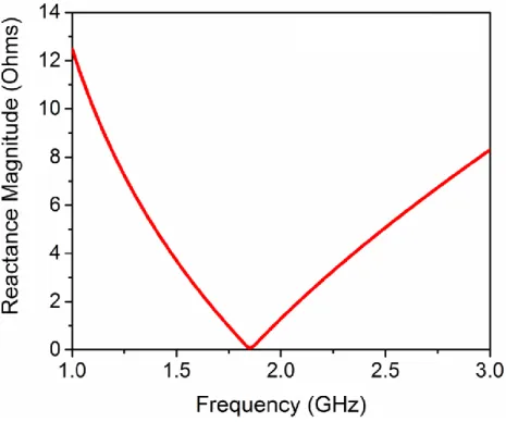
Figure 2.14. Input Reactance of the overall lumped model of the proposed antenna using NI multisim. ... 23
Figure 2.15. Radiation pattern of the proposed antenna (a) Azimuth (H-plane) radiation pattern (b) Elevation (E-plane) radiation pattern. ... 24
Figure 2.16. Received signal strength of proposed antenna. ... 24
x
Figure 3.3. (a) Fabricated antenna with ruler and the transparent antenna pattern shown in inset. (b) Partially magnified pattern showing uniform edge with 30 sec UV treatment. ... 32 Figure 3.4. (a) 3D surface profile of silver pattern deposited with 480nm thickness. (b) SEM image of silver nanoparticle ink pattern obtained with 10µm scale. ... 33 Figure 3.5. Radiation patterns of the proposed antenna (a) Azimuth pattern at
900MHz showing 16.74dBi gain. (b) Elevation radiation pattern at 900MHz. (c) Azimuth pattern at 2.4GHz showing 16.24dBi gain. (d) Elevation pattern at 2.4GHz. (e) 3D pattern at 900MHz. (f) 3D pattern at 2.4GHz. ... 34 Figure 3.6. Surface Current analysis of the antenna (a) at 900MHz and (b) 2.4GHz.35 Figure 3.7. (a) Measurement setup for reflection coefficient. (b) Setup for flexibility test with cylinder of 5.86cm radius. ... 36 Figure 3.8. Measured and simulated reflection coefficients of the proposed dual band antenna. ... 36 Figure 3.9. Reflection coefficients measured with 5.86cm radius bending and with complete folding. ... 37 Figure 4.1. The proposed inset microstrip patch antenna based on PDMS/ITO. (a) Antenna geometry for design and simulation. (b) Fabricated antenna flat and its flexible view (inset). ... 40 Figure 4.2. Material and fabrication process. ... 42 Figure 4.3. Simulated radiation patterns of the proposed inset microstrip patch
antenna. (a) E-plane radiation pattern. (b) H-plane radiation pattern. ... 43 Figure 4.4. Reflection coefficient of the proposed antenna (a) Comparison of
measured and simulated reflection coefficient. (b) Measured reflection coefficient along bending from 2 cm to 10 cm. ... 45 Figure 4.5. Transmittance of the light through the proposed antenna thickness
measured by utilizing UV visible spectrophotometer. ... 46 Figure 4.6. Restoration (to initial position) time vs bending diameter (as shown in inset of Figure 4.4). ... 46 Figure 5.1. (a) Liquid sensor design. (b) Patch Radiator with parameters. ... 50 Figure 5.2. Reflection coefficient analysis of the sensor against substrate height. ... 51
xi
Figure 5.3. (a) Reflection coefficient analysis of the sensor against design frequencies showing minimum, average and maximum reflection coefficients of consider liquids water, ethanol, oil and empty case. (b) Minimum, average and maximum frequency separation among the considered cases water, ethanol, oil and empty for different design frequencies. ... 52 Figure 5.4. Reflection coefficient of the proposed sensor with water, ethanol, oil, empty and water/ethanol 50:50 mixture. ... 54 Figure 5.5. Printing setup of Dimatix Material Printer (DMP-3000). ... 55 Figure 5.6. (a) Fabricated radio frequency liquid sensor. (b) Sensor with inlet and outlet. ... 55 Figure 5.7. (a) 3D nano profile of liquid sensor. (b) SEM image of the printed silver ink pattern. ... 56 Figure 5.8. Reflection coefficient of various liquids over 1.4 GHz to 3 GHz range and inset shows the experimental setup for measurement using vector network
xii
Table 2.1. Design parameters of antenna. ... 12
Table 2.2. Maximum antenna gains at different turns ... 17
Table 2.3. Maximum gains over different vertical lengths. ... 18
Table 2.4. Comparison of different flexible antenna with the proposed antenna. ... 25
Table 3.1. Design parameters of the proposed antenna. ... 30
Table 4.1. Simulation and design parameter of the proposed antenna. ... 41
Table 5.1. Design parameters of the proposed antenna. ... 53
Table 5.2. Summary of measured highest dip point frequency (GHz) and reflection coefficient (dB) for various liquids ... 57
xiii
List of Content
Abstract…………..………..………xv
Chapter-1 Introduction ... 1
1.1 Background ... 1
1.2 Evolution in Printed Antennas ... 2
1.3 Printing Technologies for Printed Antennas ... 3
1.4 Inkjet Printing Technology for Antenna Printing ... 4
1.5 Future Trends and Challenges of Printed Antennas ... 5
1.6 Author’s Contribution and Thesis Organization ... 6
1.6.1 Contributions ... 6
1.6.2 Thesis Organization ... 7
Chapter-2 Single band Monopole Antenna ... 9
2.1 Introduction ... 9
2.2 Antenna Design ... 10
2.2.1 Equivalent circuit design ... 11
2.2.2 Analysis of straight and meander designs ... 14
2.2.3 Analysis of right turn position variation ... 15
2.2.4 Analysis of vertical length variation ... 17
2.3 Fabrication Process ... 19
2.4 Characterization ... 21
2.5 Results and Discussion ... 22
2.6 Summary ... 26
Chapter-3 Flexible Dual-band Antenna ... 27
3.1 Why flexible dual-band antenna? ... 27
3.1.1 Introduction ... 27
3.2 Antenna Design ... 28
3.3 Experiment ... 31
3.3.1 Material ... 31
3.3.2 Fabrication Process ... 32
3.3.3 Surface Morphological Characterization ... 32
xiv
Chapter-4 Transparent Antenna ... 38
4.1 Transparent Antennas ... 38
4.2 Microstrip Design... 39
4.3 Material and Methods ... 41
4.3.1 Material ... 41 4.3.2 Fabrication ... 41 4.4 Characterization ... 42 4.4.1 Electrical Characterization ... 42 4.4.2 Optical Characterization ... 42 4.4.3 Mechanical Characterization ... 43
4.5 Results and Discussions ... 43
4.6 Summary ... 47
Chapter-5 RF Liquid Sensor ... 48
5.1 Introduction ... 48
5.2 Sensor Design... 49
5.3 Sensor Fabrication and Characterization ... 54
5.4 Results and Discussions ... 56
5.5 Summary ... 58
Chapter 6 Conclusions and Future Work ... 59
6.1 Overview and General Conclusions ... 59
6.2 Future Work ... 61
Annex-A Journal Papers ... 63
Annex-B to be Submitted Papers ... 64
Annex-C Conference Papers and Posters ... 65
xv
Abstract
In future, flexible electronic devices requires connectivity on Bluetooth, WLAN, 2G, 3G and 4G-LTE standards and need support of printed flexible single and multiband antennas. Therefore, flexible and bendable antennas are necessary and unavoidable. The nature of flexible technologies dictates that the antenna should be flexible as well as mechanically robust such that it can tolerate high level of bending, rolling and flexing repeatedly. These challenges should be addressed because the performance of printed antennas degrades due to deformation in the flexible substrate under severe conditions. Therefore, it is critical and important to study and analyze the printed antennas for flexible electronic devices.
The printed antennas can act as a radio frequency (RF) sensor to measure the permittivity of the liquids which can significantly detect the materials so, it is also important to analyze these printed antenna designs for RF sensors.
To address future challenges of flexible antennas, this thesis presents various single and dual band flexible printed antennas on transparent substrates with different geometries for wearable electronic devices. In last decade, printing technologies such as screen printing, electrohydrodynamic (EHD) and inkjet printing are attractive pattering techniques which are gaining much interest for mass fabrication of various wearable electronics devices. The tremendous interest in these technologies is due to their features of one-step manufacturing process and vacuum free processing that fulfills the realization of eco-friendly, low-cost and flexible electronic devices and systems. New organic and inorganic solution processed materials are improving the performance of the electronic devices. By utilizing the solution process materials and printing technologies, this thesis addresses the challenges of flexible antennas and RF sensor on transparent substrates.
Initially, a flexible single band monopole antenna design is presented for 1.8 GHz applications. The design of single band antenna is 2D projection of 3D helical antenna with a single turn as the 3D structures cannot be embedded in 2D flexible substrate. The mathematical modeling of the single band antenna design is presented. By using transmission line theory, the circuit model is presented which endorses the design of single band antenna and well matched with the simulation results in both circuit and
xvi
with other reported antennas is also presented. To confirm the reception capability of single band antenna, it was characterized on spectrum analyzer which showed the reception of single desired band. The antenna worked well and fully operational during flexibility test as the measured reflection coefficient was under -10 dB.
A dual-band antenna design is described on a thin flexible and transparent Polyethylene Terephthalate (PET) substrate and characterized for wearable RF electronic applications. For printing both single and dual band antennas, the conductive ink based on Silver Nano Particles (SNPs) is utilized. The flexible antenna was fabricated on a very thin 40 micron substrate through inkjet material printer. To fabricate an optimal antenna on a thin substrate, the systematic procedure is given in detail. The results of fabrication process are confirmed through surface characterizations of the fabricated antenna.
Next, a flexible and transparent inset-microstrip patch antenna based on conductive indium tin oxide (ITO) is presented. The patch antenna is fabricated on a Polydimethylsiloxane (PDMS) substrate and characterized with the help of Agilent network analyzer. The bendability and transparency tests are given for transparent wearable RF electronic applications. The presented flexible antenna design shows excellent performance over the considered band. Therefore, the proposed design provides an RF industrial solutions for future low-cost, eco-friendly and flexible wearable electronic market.
Finally, a microstrip patch RF sensor is demonstrated for liquid identification. The relationship between the dielectric constant and resonance frequency provides the liquid sensing mechanism. The design procedure is given to find not only maximum frequency separation between two adjacent resonance frequencies but also lowest reflection coefficients at the resonance frequencies for all considered liquids. The fabricated sensor has 140 MHz minimum frequency separation and maximum -29 dB reflection coefficient, which gives large identification margin. By comparing with the existing sensors, the RF liquid sensor exhibits outstanding identification capability. Therefore, this type of patch sensor can be utilized in RF tunable liquid detection applications.
Chapter-1 Introduction
1
Chapter-1
Introduction
1.1 Background
Antenna technology is used in many electronic applications such as Wireless Fidelity (Wi-Fi), Bluetooth, Zig-bee, mobile phones, satellite communication, Radio Frequency Identification (RFID), Global Positioning System (GPS) and telemedicine radio, to facilitate the daily life. An important category in antenna technology is flexible and wearable antennas which have gained more attention from both industry and academia. The popularity and demand of flexible antennas increased because of recent advancement in the field of printed electronics. In recent years, the printed electronics has emerged as a new branch of electronics where functional materials are directly deposited through numerous printing techniques on inexpensive flexible plastic films or substrates, to make operational electronic devices and systems [1]. The electronics market analysis indicated that the estimated revenue of printed electronics is going to be 30 billion US dollars and, it will increase above 300 billion US dollars by the end of 2028 [2].
This tremendous amount of market share shows the demand and popularity of printed electronic. Consistently, the flexible electronics systems and devices often needs the integration of flexible antennas operating in the desired frequency bands to provide wireless connectivity. However, the new electronic applications impose severe limitations to meet their demands, especially which requires mechanical flexibility and compatibility with flexible electronic circuits and systems. Conventional manufacturing techniques comprises on vacuum processing and a series of thin layer film deposition steps such as coating, photoresist, etching and again photoresist peel off to transfer the pattern on the thin film. This process also involves a large waste of materials that increases the overall processing and device cost. On contrary, we can fabricate the low cost electronic devices by utilizing techniques such as inkjet, gravure and offset printing which deposit the right amount of material on the required place and there is no wastage of material in fabrication process. Furthermore, it fulfills the missing gaps of conventional lithographic process with environmental friendly, low
2
temperature and ambient conditions processing. Printing industry that involves offset, inkjet printing and Roll to Roll (R2R) printing processes have shown extremely fast printing of electronic circuit as meters per minute that is almost competitive to the vacuum based fabrication techniques [3].
The flexible antennas can be fabricated by using flexible polymer, plastics, polyester, polyethylene and paper as a substrate and conductive solution processed materials as an active material [4]. The substrates are low-cost, energy efficient, lightweight and compatible with large area manufacturing by utilizing R2R and also small area development is possible through sheet-to-sheet fabrication technique [5]. These substrates are the perfect complement to be used with printing technologies, rather than with standard clean-room techniques such as photolithography, lift-off or etching. From this point of view, the term flexible printed antennas often implies the use of a plastic, textile or paper substrate. In short, all the advantages of printed techniques over conventional manufacturing techniques make the flexible antenna as an attractive candidate for the future consumer Radio Frequency (RF) electronic market. Some of the printed antennas are shown in Figure 1.1.
Figure 1.1. Printed flexible antennas [5], [6].
1.2 Evolution in Printed Antennas
Previously, the antennas were printed on a rigid Flame Resistance-4 (FR4) substrate to provide the wireless connectivity to the printed circuits and systems [7]. However, flexible electronics technology is one of the popular trends in modern world. To provide wireless connectively in specific frequency band over wireless networks, the vast majority of flexible electronic circuits and systems need integration of flexible
Chapter-1 Introduction
3
antennas. This is the necessity of today’s information oriented society. The efficiency and performance of the printed electronic systems depends on the efficiency of the integrated antenna. Hence, the desired flexible antenna can not only capable of meeting the flexible wireless connectivity demands such as low-cost, compact, lightweight, low profile and mechanically robust but, also it should be efficient with desired bandwidth and radiation characteristics. To design a high functional flexible printed antenna particularly for small devices is challenging task because of its integration in a very compact size. A compact flexible and transparent antenna is needed for integration with future printed wearable electronics devices operating over the required frequency bands [8]. Therefore, an urgent demand for low-cost, fast, efficient, high-precision and reliable fabrication, exists. The task can be tackle by applying the printing technology for flexible antennas. The next section presents the available printing technologies for antenna fabrication.
1.3 Printing Technologies for Printed Antennas
Recent years have seen a great demand in the field of flexible printed antennas because of their light weight, environment-friendly, low-cost manufacturing and ease of fabrication. The availability of inexpensive substrates such as papers, textiles, and plastics make flexible printed antenna an attractive candidate for the next generation of consumer electronics systems. This section describes the current available printing technologies for the fabrications of wearable flexible antennas. Among these available methods, some are matured and commercialized whereas some techniques are still under research. The key task of the printing technique is to deposit the functional active materials on the flexible substrate with high accuracy and uniform film thickness. In history, various thin films deposition techniques have been adopted that includes chemical bath, slot casting, spin-coating, spray coating, dip coating, screen printing, doctor blade, inkjet printing, metering rod and aerosol jet. Figure 1.2 shows the schematic diagrams of different printing techniques. Other printing techniques, electrostatic spray deposition (ESD) and electro hydrodynamic (EHD) are also used for the deposition of thin films, where the functional material is deposited using electrostatic field [2]. All fabrication methods have their own advantages and disadvantages.
4
Figure 1.2. Various printing techniques based on solution-processed manufacturing [2]Error!
Reference source not found..
In this thesis, ink-jet printing technique is used for the fabrication of flexible antennas and RF sensor. This technique is discussed in the forthcoming section.
1.4 Inkjet Printing Technology for Antenna Printing
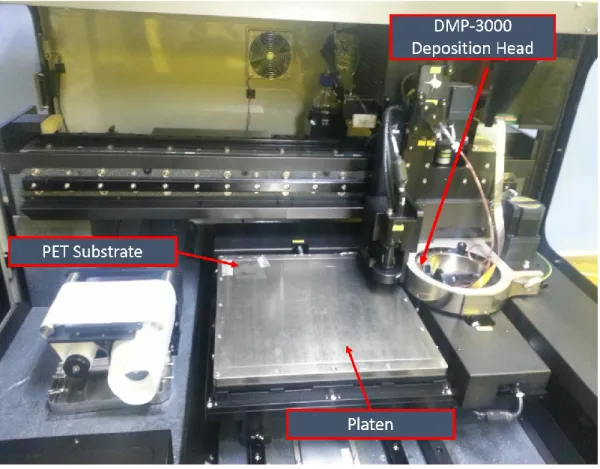
In this work, inkjet Digital Material Printer (DMP-3000) has been utilized for printing the antenna design. Digital photograph of the DMP-3000 is shown in the Figure 1.3 (a), it consists of a DMP-3000 printer and a personal computer with monitoring unit. Figure 1.3 (b) shows the schematic diagram of the DMP-300 printer. The main components are shown which includes temperature controller, camera, monitor, PC, nozzles head, ink reservoir, pressure controller, LED light and moveable stage. The DMP-3000 printer has print area of 300 × 300 mm, position accuracy of ±5 µm, repeatability of ±1 µm, and platen temperature in the range of 25 to 60 °C. To print a pattern of antenna through inkjet printer various steps are followed from design of layout to the device [9].
Chapter-1 Introduction
5
Figure 1.3. (a) Digital photograph of DMP-3000 inkjet material printer. (b) Schematic diagram of the DMP-3000 along main components [9].
1.5 Future Trends and Challenges of Printed Antennas
To meet with the demands of next generations electronic applications which are low-cost, large area, flexible and environmentally friendly, printed electronics is an attractive, appealing and emerging field. The printed electronic devices such as OLED display, RFID tags and biomedical sensors are well matured and commercialized. To communicate these flexible printed electronics devices, the integration of flexible antenna is necessary to provide wireless connectively over wireless networks. The flexible antenna should be low-cost in both materials and fabrication [5], [8].
Day by day, the demand for antennas is increasing to suit a wide variety of exciting applications such as flexible and wearable electronic sensing and wireless applications. The optimal functionality of these printed devices depends on the characteristics of the integrated antenna. The main challenge is not only to meet with the nature of requirements of printed electronics such as low-cost, flexible, compact, lightweight and environmentally friendly device but also to provide a mechanically robust and efficient solution in term of performance. The nature of flexible technologies dictates that the antenna should be flexible as well as mechanically robust such that it can tolerate high level of bending, rolling and flexing repeatedly.
There are additional challenges associated in designing the flexible antennas which do not exist when designing conventional antennas for wireless systems. The resonant frequency and return loss of the flexible antenna deteriorates and these losses should be accounted. Subsequently, flexible antennas are prone to deterioration due to
6
impedance mismatch under bent or rolled conditions. The functionality and efficiency of the antenna also degraded under these severe operation scenarios.
1.6 Author’s Contribution and Thesis Organization
1.6.1 Contributions
The main objective of thesis is to address these challenges by presenting a systematic approach that includes the design, simulation, fabrication and characterization of Nano Particles (NPs) based antennas and sensor. Moreover, the focus of this research is to develop versatile low-cost antennas and sensor by exploring new design techniques, printing technologies and functional active materials to realize the optimized eco-friendly flexible printed antenna. In this context, the research is divided into four sections which are explored step by step. In first part, innovative 2D monopole single band design which is projection of 3D helical antenna is developed with electrical conductive Silver Nano Particles (SNPs) ink and extremely flexible thin Polyethylene Terephthalate (PET) substrate. A systematic design approach with the help of transmission line theory is presented and, the design performance is confirmed through fabricated antenna. A performance comparison of the proposed SNP-based miniature printed antenna is presented with the identical printed antennas which reveals that the presented single band monopole design has excellent performance in term of gain, efficiency, compactness and robustness. In the next part, a coplanar waveguide (CPW) based high gain dual-band monopole design is presented on a very thin 0.04 mm flexible PET substrate for both radar and communication bands. The inkjet printing process is explored and analyzed on a thin substrate through SNPs based ink. The effects of printed layer thickness and number of printed conducting layers on the performance of antenna are investigated. The effect of ultra violet treatment, curing time and temperature on SNP film is examined. The film uniformity and thickness is evaluated through 3D surface morphology and Scanning Electron Microscope (SEM). A systematic procedure is presented that yields excellent fabrication which is confirmed through flexibility test. In the third section, a low-cost flexible transparent inset microstrip antenna is developed through inkjet printing technique for transparent flexible electronic applications. To design and analyzed the indium tin oxide (ITO) and Polydimethylsiloxane (PDMS) based antenna Finite Element Method (FEM)
Chapter-1 Introduction
7
formulation is implemented in High Frequency Structure Simulator (HFSS). The optical and electrical measurement performed by using Shimadzu spectrophotometer and Hewlett-Packard (HP) network analyzer, respectively. The antenna showed up to 90% transparency. In the fourth and final part of this research, a low-cost inset microstrip based RF inkjet printed sensor is developed for liquid sensing applications. The FEM based best design is achieved which can easily identifies the considered liquids as the resonance frequency separation is large and reflection coefficient is under -25 dB.
1.6.2 Thesis Organization
The thesis is organized into six chapters as follows:
Chapter 2 deals with the design, equivalent circuit, working mechanism, fabrication and characterization of single band monopole antenna on a very thin 40 micron PET substrate. The FEM based analysis of the antenna design is described in detail. The antenna is fabricated by utilizing inkjet printing technique. The electrical, mechanical and surface morphological characteristics are investigated for the fabricated devices. Chapter 3 review and describes the dual bands 900 MHz and 2.4 GHz antenna design. The working principle on both bands is done in detail. The current distributions and radiation characteristics are discussed on both operational bands. The dual band antenna design is fabricated on a very thin 40 micron PET substrate through DMP-300 inkjet material printer. The fabrication process is described in detail as it was challenging to deposit the antenna pattern of this thin hydrophobic substrate. The surface morphological, electrical and mechanically characteristics is done to show its compatibility with the wearable printed electronics applications.
Chapter 4 deals with fabrication of transparent microstrip patch antenna on a flexible and transparent PDMS substrate. The transparent and conductive ITO ink has been utilized to fabricate the patch and the ground of the antenna design. The optical transparency analysis is done that shows, the device is transparent. The electrical and mechanically performance is investigated for transparent printed wearable electronic applications.
8
Chapter 5 describes a printed RF inset-microstrip sensor for liquid identification applications. The full wave analysis is shown in detail to obtain the best sensor design in term of minimum reflection coefficient (for all considered liquids) and large resonance frequency separation among liquids. The Ag Nano Particles (AgNPs) ink is used to fabricate the liquid RF sensor through inkjet printing technique. The sensor performance is shown to distinguish various liquids including water, oil, ethanol and mixed cases.
Chapter 6 describes the conclusion of this thesis and future work.
Chapter-2 Single band Monopole Antenna
9
Chapter-2
Single band Monopole Antenna
2.1 Introduction
Nowadays, printed electronics has gained high attention due to low cost, environment friendly, and easy fabrication of electronic devices. In particular, printed antenna is common in RFID, near field communication (NFC), high frequency radio transmission and reception applications [10-15]. Printing techniques like EHD, screen printing and inkjet are low cost and have ability to deposit the material accurately on hydrophilic material substrates [16-24]. There are some substrates which are hydrophobic (like PDMS). However, the ink can be effectively deposit on these substrates with good contact angle by utilizing a small treatment such as plasma or UV [25]. Therefore, manufacturing of printed antennas is possible without high cost wet etching processes by direct printing techniques [26]. The selection of the low cost transparent and biocompatible substrate material is important to print antenna for wearable electronics devices. Recently, printed antennas on various flexible substrates, including paper, kapton and polyimide film has been reported [27-32]. Among these substrate materials, paper is low profile (with small thickness and weight) flexible and low cost substrate which is commonly used for printing antennas in printing electronic devices [31]. However, paper based opaque substrates are not robust and cannot be used in hard ambient environment. Secondly, all these substrates are mainly restricted by their high loss tangent (such as for paper tan𝛿 = 0.072 from 0.5 to 2.5GHz). Hence, low cost PET substrate is now used in many printed wearable electronic applications like OLEDs, organic thin film transistors (OTFTs) and organic memory [33-36], is a promising substrate with lower tan loss factor of 0.003 at 1 GHz [37]. Furthermore, the surface roughness of the PET is lower as compared to other substrate material like paper, which also lowers the reflection loss due to surface roughness of the substrate material [38]. Recently, a few antenna designs have been demonstrated on PET substrate [39-42] but most of the works have been carried out for prior RF characteristics to support printed antenna and also the printed designs are not compact [42]. To design high functional antennas particularly for small devices (like Teleos etc.) is a difficult and challenging task due to their integration in a very compact
10
geometry. A compact flexible and transparent antenna is needed for integration with future printed small wearable electronics devices operating over 1.8 GHz band. To apply wearable electronics devices at 1.8 GHz band, a compact printed antenna design on a fully flexible and transparent PET substrate is presented. The proposed antenna is designed by using resonant properties of printed monopole and is a variant of monopole designs presented in [30-31], [43]. The antenna is designed and simulated in general purpose computer aided design (CAD), Ansys HFSS. The simulated design is fabricated through commercial Dimatix inkjet material printer (DMP-3000) at ambient conditions, by depositing silver nanoparticle ink on a PET substrate in single step. The fabricated antenna is electrically characterized by using vector network analyzer (VNA). The measured reflection coefficient is -32.2dB at 1.8GHz and -10dB bandwidth of 190.5MHz. The practical signal strength of -60.64 dBm is received by using LG spectrum analyzer. The simulated gain of the proposed antenna is 2.72dBi and its efficiency is 93.33%. Mechanically the propose antenna is fully flexible, and optically transparent on a 40micron PET substrate. The proposed antenna geometry is simple and can be tunable to any frequency.
Figure 2.1. (a) Antenna design. (b) The equivalent electrical circuit of antenna.
2.2 Antenna Design
The geometry of the antenna as shown in Figure 2.1(a) is inspired from helical antenna. The space and number of turns in the meander pattern defines the value of inductance and capacitance [44], in this design we have used only one turn to achieve our desired
Chapter-2 Single band Monopole Antenna
11
inductance and capacitance values for 1.8 GHz band. The antenna is fed by coplanar waveguide (CPW) due to its advantage of low dispersion and low radiation leakage over simple microstrip line feed method. Secondly, CPW antenna makes antenna fabrication simple and fast as the radiating element and the ground are printed on the same side of the substrate. The basic radiating element is formed by a single right angle bend as shown in the center of Figure 2.1(a), where most radiation occurs due to
discontinuities [45]. The right angle bends are used to reduce the discontinuity susceptance which helps in impedance matching. The impact of right angled part in the antenna is acting like a load and a single turn is equivalent to an inductor. The magnetic field inside the turn is canceled out and only the horizontal parts of turns contributes in far field radiation pattern. Most of the radiation occurred at right angle bends which add up to produce desire polarization of the antenna. The considered substrate is 0.04mm thick PET whose dielectric constant is 2.8 and loss factor of 0.003 at 1GHz frequency [37]. The conductivity of silver nanoparticle ink (which is used to for radiating element) is 1.42 x 10⁵ S/m after sintering at 240°C [46]. There is tradeoff
between bandwidth and gain while increasing number of turns. The turn gap of 2.7mm is selected to lower the capacitive coupling between the radiating arms. Furthermore, the resonant frequency is directly proportional to the physical length of the antenna and shape. The straight elements L2, W4 and L4 are sensitive to resonance frequency
as they are multiple of wavelength while the transition can be adjusted.
2.2.1 Equivalent circuit design
The equivalent circuit diagram of the antenna is given in Figure 2.1(b). The shunt
conductance G1 & G2 and shunt capacitances C1 & C2 are present between antenna feed
line and ground plane through air. The silver pattern bulk resistance, inductance and capacitance are given by Req, Leq and Ceq respectively. We explain the signal
transmission from input of the antenna to the air through our antenna’s equivalent circuit. Initially, a low frequency signal is applied to the antenna, the impedance of the circuit is high due to the Ceq as capacitances are open circuit at low frequencies
(XC=1/2πfC). In this case the signal is dropped on the circuit and do not flow to the
air. On the other hand, when a high frequency signals is applied to the input of antenna, the impedance of the antenna becomes high due to the reactance of Leq (XL= 2πfL). In
12
reactance is equal to the capacitive reactance and they cancel each other. In this case, the total impedance of the circuit is equal to the Req which indicates low impedance
hence, maximum signal passes through the circuit. Using the analogy of the electrical equivalent circuit, only certain frequency band passes to the air and rest of the frequencies are reflected back to the source due to mismatch of the impedance. The proposed antenna geometry is optimized in terms of resonance frequency, gain and size as described in sections 2.2.2, 2.2.3 and 2.2.4. The geometry design has a significant impact on the performance of the antenna as described in detail in section 2. The dimensions of the proposed antenna are given in Table 2.1.
Table 2.1. Design parameters of antenna.
Parameter Dimension (mm) Parameter Dimension (mm) L1 4.05 L3 8.14 W1 4.05 W3 1.35 L2 15.8 L4 22.75 W2 5.4 Tg 9.49
The antenna structure is a combination of straight line segments and bending segments. The line segments are considered as distributed transmission line [44], [47]. The lumped parameter equivalent for straight transmission line segments is represented by T-equivalent network as shown in Figure 2.2 (a) where Z1 is defined by the following
equation.
𝑍1 = 𝑗𝑍𝑜tan(𝛽𝑙) (1)
Here, = 2𝜋/𝜆𝑒𝑓𝑓 , and 𝜆𝑒𝑓𝑓 = 𝜆𝑜
√𝜀𝑒𝑓𝑓 , 𝜆𝑜= 𝑐/𝑓 and 𝜀𝑒𝑓𝑓 is given by,
𝜀𝑒𝑓𝑓 =𝜖𝑟+ 1 2 + 𝜖𝑟− 1 2 √ 1 1 +12ℎ𝑤
Chapter-2 Single band Monopole Antenna
13
where 𝜖𝑟 represents the relative permittivity of the substrate and h is the height of the substrate.
Figure 2.2. (a) Equivalent T-network. (b) Lumped model of right angle bend.
In equation (1) Z0 represents the characteristic impedance of the transmission line and
is given by the following relationship [43],
𝑍0 = 276 log (2𝑠 𝑤)
where s is the spacing between turns and w is the track width of transmission line. The second impedance Z2 is given by the following equation,
𝑍2 = − 𝑗𝑍𝑜
tan(𝛽𝑙) (2) As tan (𝑥) ≈ 𝑥 and sin (𝑥) ≈ 𝑥 for 𝑙 ≪ 𝜆𝑔. Using this approximation 𝑍1 in equation (1) becomes inductive reactance as 𝑍1 = 𝑗𝑍𝑜𝛽𝑙 while 𝑍2 in equation (2) becomes
capacitive reactance as 𝑍2 = −𝑗𝑍𝑜𝛽𝑙.
By comparing 𝑍1 with inductive reactance 𝑍1 = 𝑗𝜔𝐿𝑙 and 𝑍2 with capacitive
reactance 𝑍2 = 1/𝑗𝜔𝐶𝑙, and using Z0 and 𝛽, yields the following expressions to
calculate the inductance and capacitance (per unit length) of the straight line segments respectively.
𝐿 = 𝑍𝑜√𝜀𝑒𝑓𝑓 𝑐
14 𝐶 =√𝜀𝑒𝑓𝑓
𝑐𝑍𝑜
The overall lumped inductance and capacitance of the structure is given by 𝐿1 = 𝐿𝑙
and 𝐶1 = 𝐶𝑙 respectively. Where 𝑙 represents the length of line segment.
The bending line segments can be represented by T-network with inductance and capacitance as shown in Figure 2.2 (b). The charge accumulates at the corners (bents)
which creates capacitance while, the interruption of current at the corner produce inductance. The bending inductance and capacitance is given by [48].
𝐶𝑏 𝑤 = (9.5𝜖𝑟+ 1.25)w ℎ + 5.2𝜖𝑟+ 7 [ 𝑝𝐹 𝑚] , [ 𝑤 ℎ > 1] 𝐿𝑏 𝑤 = 100 (4√ 𝑤 ℎ − 4.21) [ 𝑛𝐻 𝑚]
Where Cb and Lb are bend capacitance and inductance respectively. There might be
fringing field at the end of the structure but as the ground and end of the transmission separation is large. Hence, the open ended capacitance can be neglected. The overall lumped equivalent circuit is given in Figure 2.3.
Figure 2.3. The overall lumped circuit of antenna.
2.2.2 Analysis of straight and meander designs
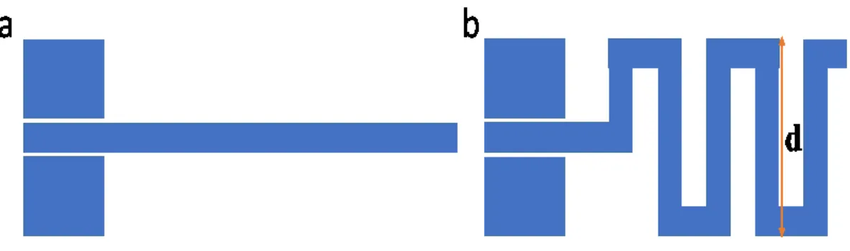
We have analyzed two extreme antenna designs as shown in Figure 2.4 (a) and (b). For
Chapter-2 Single band Monopole Antenna
15
Figure 2.4. (a) Straight Geometry (b) Meander type bending geometry.
With straight design, we obtained gain of 2.5dBi and resonance frequency of 1.8GHz. With the meander design as shown in Figure 2.5, we obtain 3.2dBi increased gain and
shifted resonant frequency of 2.55GHz. The increase of resonant frequency is due to turns (discontinuities) causing more radiations.
Figure 2.5. Reflection Coefficient of straight and meander type shapes
2.2.3 Analysis of right turn position variation
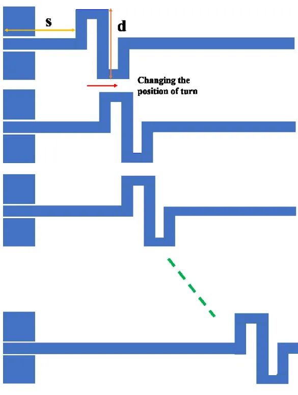
We analyzed antenna radiation characteristics by changing right turn position labeled as S in Figure 2.6. For analysis, we fixed d, height of the turn.
16
Figure 2.6. Right angle turn position variation along horizontal axis.
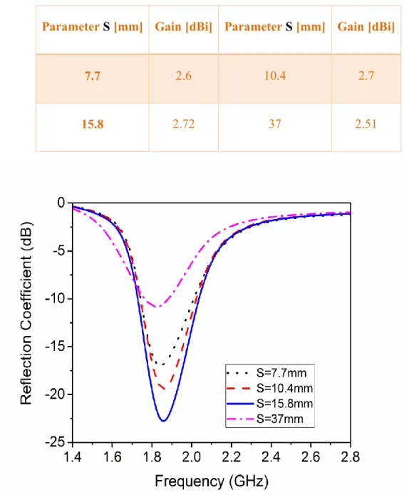
As shown in Figure 2.7, shifting the turn position near to ground causes more capacitive
coupling and resonant frequency is slightly changed from 1.84GHz to lower frequency. However, shifting the turn position to right, does not cause shift of the resonance frequency of 1.84GHz and cause change of the reflection coefficient resulting in input impedance change. The maximum antenna gains at different positions of turns are summarized in Table 2.2.
Chapter-2 Single band Monopole Antenna
17
Table 2.2. Maximum antenna gains at different turns
Parameter S [mm] Gain [dBi] Parameter S [mm] Gain [dBi]
7.7 2.6 10.4 2.7
15.8 2.72 37 2.51
Figure 2.7. Reflection coefficients at different value of S.
2.2.4 Analysis of vertical length variation
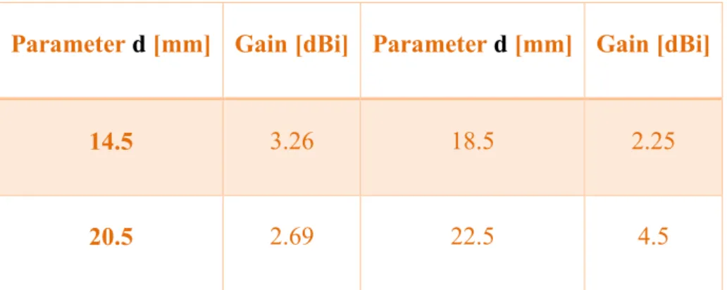
With fixed antenna pattern length, we analyzed characteristics corresponding to variation of vertical length denoted as d in Figure 2.8. As d increased, antenna gain increased and the resonance frequency was changed from 1.8GHz to higher frequency as shown in Figure 2.9. The resonance frequency was shifted from 2.3GHz to 1.98GHz
as d decreased from 22.5mm to 14.5mm. The maximum antenna gains against different values of d are given in Table 2.3.
18
Table 2.3. Maximum gains over different vertical lengths.
Parameter d [mm] Gain [dBi] Parameter d [mm] Gain [dBi]
14.5 3.26 18.5 2.25
20.5 2.69 22.5 4.5
Chapter-2 Single band Monopole Antenna
19
Figure 2.9. Reflection coefficient against vertical length variations.
The radiation of the antenna is highly dependent on the length of first transition and it needs to be longer enough to allow good wave conformation but increases the antenna size.
2.3 Fabrication Process
The proposed antenna was designed and simulated by HFSS and exported to ACE 3000 software that converted the design file into bitmap format with all geometrical information. Then the bitmap file was converted into Inkjet printer supported file format by Dimatix Drop Manager (DDM). Before initialization of printing process, silver nano particles ink (3ml), purchased from ANP South Korea, was filled into cartridge of 16 nozzles with diameter of 50µm and distance between nozzles is 254µm. Single drop of 10pl is selected for printing the proposed antenna pattern on a commercial 40-micron thick, flexible and transparent PET substrate purchased from sigma Aldrich. The low-cost PET substrate has good mechanical and thermal characteristics in polyamides and it can withstand up to 200 °C. Prior to printing, we cleaned the PET with ethanol at ambient conditions and then rinsing with distilled water and dry it at 50°C for 5 min, to remove scratches and contamination on the PET surface. Then we deposited the antenna pattern over the PET substrate. Due to
20
hydrophobic nature of the substrate, the silver nanoparticle ink was scattered over the PET surface. To resolve spreading and scattering of silver ink on the surface, experimentally we obtained that UV treatment of 30s produces optimum result. This process makes the substrate surface slightly rough and avoids random spread of silver nanoparticles over the surface. Finally, the UV treated PET was placed onto the plate of material inkjet printer, as shown in Figure 2.10 for printing antenna pattern.
Figure 2.10. Direct printing of the antenna on PET substrate using Dimatix Inkjet Material Printer.
The proposed antenna was printed on the PET substrate by AgNPs ink and thermally treated with hot platen for 15min at 70°C. The curing was done immediately after the printing process since the AgNPs ink is easily oxidized, which results in poor radiation efficiency. After printing process, the SMA connector was attached to the printed antenna by using silver nanoparticles conductive epoxy paste and then antenna was cured at 50 °C for 2h. The resultant antenna is shown in Figure 2.11 (a) and transparency as well as flexibility with low thickness of 0.04mm can be observed in Figure 2.11 (b).
Note that the fabricated antenna can be mounted on Telos-B as shown in inset of Figure 2.11 (b).
Chapter-2 Single band Monopole Antenna
21
Figure 2.11. Proposed fabricated printed antenna on a PET substrate (b) Transparent and flexible PET (with 0.04mm thick) based printed antenna mounted on Telos-B (inset).
2.4 Characterization
Field Emission Scanning Electron Microscope (FESEM) image of the printed antenna pattern, as shown in Figure 2.12, which clearly shows that the gaps between silver nanoparticles are diminished due to high temperature and long curing time. The SEM image also assures formation of solid metal conductive printed track, which provides percolation channel flowing conduction electrons.
22
The electrical characteristics of antenna under test (AUT) are measured by two port calibrated HP VNA that is connected with 50Ω transmission line and 50Ω RF SMA connector as shown in Figure 2.13 (a). The bendability and flexibility tests have been
carried out by bending the AUT over radii of 2.5cm and 3.25cm. The received signal strength of AUT is measured by connecting the AUT with SA-7270 9KHz-2.7GHz LG spectrum analyzer.
Figure 2.13. (a) Measured Reflection coefficient using HP vector network analyzer. (b) Measured (over different bending radii) and simulated reflection coefficient for the proposed printed antenna.
2.5 Results and Discussion
The proposed antenna performance was verified by simulation and measurement of resonance, gain, efficiency, reflection coefficient and received signal strength. The overall lumped circuit shown in Figure 2.3 has inductance and capacitance of 0.7nH and
11 pF, respectively. The input reactance of the circuit model is shown in Figure 2.14 ,
indicating resonance at the desired 1.8 GHz. The simulated radiations patterns of elevation (E-plane) and azimuth (H-plane) radiation patterns are shown in Figure 2.15
(a) and (b), respectively. The simulated gain at 1.84 GHz resonant frequency is 2.72 dBi, which is reasonable as compared to other printed antennas [10-14], [30-31]. The simulated directivity at 1.84 GHz is 3.02 dBi and then total efficiency becomes -0.3 dB, which results in 93.33% efficiency. The front to back (F/B) ratio of 0.48 dB is observed in both elevation plane and azimuth planes, indicating that the proposed antenna is omnidirectional antenna. Also, we investigated the antenna performance
Chapter-2 Single band Monopole Antenna
23
under extreme cases of the straight and complete meander type bending shapes. When the antenna completely bended in meander type shape, the resonance of the antenna was changed from 1.8GHz to 2.5GHz and gain was increased to 3.2dBi. However, in straight case the resonance was remained at 1.8GHz and 2.5dBi gain was observed. Similarly, the turn position and vertical length variations has been analyzed. The value of reflection coefficient was changed due to impedance mismatch however, the resonance and the gain of antenna were almost remained same in turn position analysis. While in vertical length variation resonance frequency as well as gain of the antenna changed (see section 2.2.3 for detail).
Figure 2.14. Input Reactance of the overall lumped model of the proposed antenna using NI multisim.
The electrical characteristics of antenna under test (AUT) are measured by two port calibrated HP VNA that is connected with 50Ω transmission line and 50 Ω RF SMA connector as shown in Figure 2.13 (a). The measured and simulated reflection
coefficients (S11) are shown in Figure 2.13 (b), in which we can observe that the
measured resonant frequency is 1.84 GHz and the measured S11 is agreed with the
simulation result. The measured -12 dB bandwidth is 280MHz (∆fBw= 15.56%) and the received signal strength measured by connecting the AUT with SA-7270 9KHz-2.7 GHz LG spectrum analyzer is -60.64 dBm at 1.84 GHz. This received signal
24
strength is consistent under background noise at 1.84 GHz as shown in Figure 2.16.
Thus implies that the designed antenna can operate at real-world application using 1.84 GHz band.
Figure 2.15. Radiation pattern of the proposed antenna (a) Azimuth (H-plane) radiation pattern (b) Elevation (E-plane) radiation pattern.
Figure 2.16. Received signal strength of proposed antenna.
The bendability and flexibility tests have been carried out to investigate the performance of the antenna under deformation. Bending of antenna causes change of resonance frequency as well as the reflection coefficient and impedance mismatch due
Chapter-2 Single band Monopole Antenna
25
to change in its effective length. Reflection coefficient was measured by bending the AUT over radii of 2.5 cm and 3.25 cm. Consequently, the reflection coefficient decreases and resonance frequency shifted from 30-60 MHz to higher frequency under convex bending as shown in Figure 2.13. Even the reflection coefficient degraded with
bending, AUT performed well since the reflection coefficient was still less than -10 dB.
After restoring to its original position, no permanent deformation and deterioration has been observed. The performance was not deteriorated during bending experiments, carried out more than hundred times.
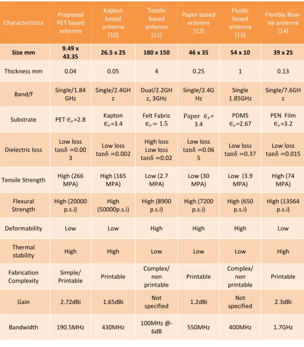
Table 2.4. Comparison of different flexible antenna with the proposed antenna.
Characteristics Proposed PET based antenna Kapton based antenna [10] Textile based antenna [11] Paper based antenna [12] Fluidic based antenna [13] Flexible Bow-tie antenna [14] Size mm 9.49 x 43.35 26.5 x 25 180 x 150 46 x 35 54 x 10 39 x 25 Thickness mm 0.04 0.05 4 0.25 1 0.13 Band/f Single/1.84 GHz Single/2.4GH z Dual/2.2GH z, 3GHz Single/2.4G Hz Single 1.85GHz Single/7.6GH z Substrate PET ∈𝑟=2.8 Kapton ∈
𝑟=3.4 Felt Fabric ∈𝑟= 1.5 Paper ∈𝑟= 3.4 PDMS ∈𝑟=2.67 PEN Film ∈𝑟=3.2 Dielectric loss Low loss tanδ =0.00 3 Low loss tanδ =0.002 High loss Low loss tanδ =0.02 Low loss tanδ =0.06 5 Low loss
tanδ =0.37 tanδ =0.015 Low loss
Tensile Strength High (266 MPA) High (165 MPA) Low (2.7 MPA) Low (30 MPA) Low (3.9 MPA) High (74 MPA) Flexural Strength High (20000 p.s.i) High (50000p.s.i) High (8900 p.s.i) High (7200 p.s.i) High (650 p.s.i) High (13564 p.s.i)
Deformability Low Low High High High Low
Thermal
stability High High Low Low Low High
Fabrication Complexity Simple/ Printable Printable Complex/ non printable Printable Complex/ non printable Printable
Gain 2.72dBi 1.65dBi Not
specified 1.2dBi
Not
specified 2.3dBi
Bandwidth 190.5MHz 430MHz 100MHz
26
The proposed antenna is comparatively analyzed, as shown in Table 2.4, with different flexible antennas presented in [10-14]. The antenna is analyzed on the basis of electrical and mechanical properties. The main focus of this comparative analysis is on compactness and robustness. Flexibility, deformability, thermal stability and tensile strength are the major mechanically properties considered to investigate the robustness of the proposed antenna. Fabrication process and its complexity are also included in this analysis. Table 2.4 shows that the proposed antenna design is relatively compact,
fully flexible, robust and small in loss factor (tanδ). The gain of the presented antenna is high as compared to other printed antennas, whereas the bandwidth is relatively small. The simple fabrication process on a low-cost PET substrate allows industrial roll to roll (RoR) production and also, further weight reduction for antenna integration with RF IC.
2.6 Summary
We proposed a novel ink-jet printed antenna on 40 micron thick, flexible and transparent PET substrate for 1.8 GHz band applications. The antenna was designed and simulated via HFSS and was verified through NI Multisim simulation using equivalent circuit model. The proposed antenna has achieved gain and efficiency of 2.72 dBi and 93.33% respectively. The antenna was realized with commercialized DMP-3000 by depositing silver nanoparticles ink as radiating element and ground on the UV treated PET substrate. The fabricated antenna has shown reflection coefficient of -32.2 dB at 1.84 GHz band which agrees with simulation result. These results indicates that the proposed antenna can be used for transparent and flexible wearable electronic devices using 1.8 GHz band.
Chapter-3 Flexible Dual-band Antenna
27
Chapter-3
Flexible Dual-band Antenna
3.1 Why flexible dual-band antenna?
3.1.1
Introduction
Nowadays, Wi-Fi communication is popular since it is the most common standard for wireless communication operating in free industrial, scientific and medical (ISM) band. The standard Wi-Fi protocols of IEEE 802.11b and 802.11g use 2.45 GHz, while the IEEE802.11ah utilizes 900 MHz [49-50]. The electronic devices for all Wi-Fi protocols need integration of low-profile and low-cost dual band antenna [30]. Conventional manufacturing technology based on lithography can produce device with high accuracy. However, this fabrication process is quite complicated, time consuming and requires precise control of temperature and pressure. Other drawbacks are throughput limitations, lack of batch processing and use of rigid substrates and corrosive chemicals [3], [33], [36], [38-39].
Recently, printed electronics technology has emerged as a promising technology and widely investigated as the technology is low-cost, handy, and can operate with immediate and single-step process. The printed electronics has been used for mass production of low-cost and flexible electronic devices such as RFID antennas, OLEDs, OTFTs and organic memory [3], [33-34], [36].
Many researchers have utilized the printed electronics for antenna design and used gold and copper to achieve good radiations [36]. However, gold and copper having high curing temperature, cannot easily be printed on flexible polyamide substrate [39-40]. On the other hand, common nanoparticle ink of silver (Ag) becomes suitable for fabrication of low-cost flexible antennas since its melting temperature is low and compatible with flexible polyamide film and paper substrates.
The use of low-cost flexible substrate with low loss factor such as paper, Kapton and polyimide film have been reported [27], [30-33]. Common paper substrate has high tangent loss factor of 0.065 yet it cannot withstand hard environmental conditions. Kapton and polyamide substrates provide cost effective solution for Roll-to-Roll (R2R) mass production and also they are foldable, bendable and transparent [27],
[30-28
33]. Polyethylene terephthalate (PET) is thin, flexible, foldable and transparent. The glass transition temperature of PET is in the range of 80~100 °C so that PET is mostly used for synthetic fiber and liquid or food container [13]. Printed electronic devices and R2R processing using PET have been reported [3],[33], [34],[36], [38].
The surface roughness of PET is lower than paper and Kapton so that PET has small reflection loss [38]. The tangent loss of PET is as low as 0.003 at 1 GHz [53] so that it is adequate for high frequency applications. Antenna designs on PET substrate have been demonstrated and cost-effective and inkjet-printable antennas on PET have been developed [38-40], [54-55]. Flexible antenna on PET for single 1.8 GHz band has been reported [56]. This antenna was designed for such small device as TelosB and yet antenna gain was as low as 2.7 dBi. A dual band antenna based on Yagi log-periodic dipole array (LPDA) for wireless communication was reported [57]. The LPDA antenna was fabricated on 1 mm thick PET and designed for both WLAN-UHF band (2.4~2.5 GHz) and WLAN-SHF (5.2~5.8 GHz) band. The gain of the LPDA printed on 111.98 mm × 55 mm substrate, were reported as 5.5 dB at WLAN-UHF band and 6 to 7 dB at WLAN-SHF band.
In this paper, we propose a compact patch antenna, which has high gain and operates on dual Wi-Fi band of 900 MHz and 2.4 GHz. The proposed antenna is printed on 50-micron thickness PET substrate so that it is fully transparent and suitable for wearable devices. For antenna design, we use the HFSS and for antenna fabrication, we use commercial DMP-3000 printer by depositing AgNPs on PET substrate. Through simulations and experiments, we proved that the proposed antenna has high gain at dual bands and that is robust to severe bending and folding of antenna.
3.2 Antenna Design
The antenna structure is comprised of Z-shaped radiating monopole element fed by co-planar waveguide (CPW). The CPW feeding technique not using via-hole connection or shorting pins, has key advantage that radiating body and ground plane can be printed on the same side of substrate. This significantly reduces production cost since printing process becomes fast, simple and roll-to-roll production is possible. Furthermore, it has low radiation loss, improved impedance matching and larger bandwidth as well. The size of the antenna is minimized by adopting ring (Z) based winding, which provides longer path for current flow and minimizes significant effect
Chapter-3 Flexible Dual-band Antenna
29
on radiation pattern. We obtained optimum separation between the radiating arms (Ws)
as 9mm, which matches with 50 ohms input and reduces coupling effect between arms as well. The smaller separation than 9mm increases coupling effect and hence, degrades the antenna performance of impedance matching. The Z-shape monopole antenna fed by 3.5 mm wide CPW is printed on same side of the substrate. Contrary to the dipole antenna, the monopole antenna uses its ground as radiating surface and prevents the antenna from external electronic circuit effects as current leakage and electrical surge etc.
Figure 3.1. Geometry of antenna
To achieve dual band characteristics, we adjust length Ls and width Ws of the rectangular slots inside the L × W rectangular monopole. The Ls is adjusted for radiation at specific band and the number of transition is adjusted for bandwidth and gain requirement of the band. Note the antenna has two current flows i.e. longer path and shorter path. The longer meander type path has total length of 151.61mm (Lf + Wf/2 + W/2 + 2Ws + 2W), which is approximately equal to one-half wavelength of 900MHz. Similarly, the shorter path has total length of 61.61mm (Lf + Wf/2 + W/2), which is approximately equal to one-half wavelength of 2.4GHz. Consequently, the proposed antenna structure produces dual resonant modes. Increasing the size of the
30
ground slightly increases directivity of antenna with the expense of size increment. The distant (d) between the radiating element and the ground give primary influence on both radiation pattern and antenna impedance. Radiation of antenna highly depends on the length of first transition so that it should be separate enough to allow good wave conformation into free space.
Using these design considerations, we obtain the size of monopole antenna as 45mm × 36 mm and the size of two rectangular slots as 27 mm × 9 mm (symmetric on both edges), which are inserted into the monopole for both impedance matching and radiation at dual bands. The resultant Z-shape antenna is as shown in Figure 3.1 and the
parameters are given in Table 3.1. To print the antenna, we deposit the AgNPs on 86.9 mm × 54.7 mm PET substrate, which is transparent, flexible, 0.05 mm thick, dielectric constant of 2.8 and loss tangent of 0.003 at 1GHz frequency [53]. Note that the proposed design has L × W rectangular structure containing two Ls × Ws symmetric slots inside the structure, which has dual band characteristics differentiating the single band antenna [56] having straight line and meander geometry in the middle. In addition, the proposed dual band antenna has much higher gain than the antenna in [56].
Table 3.1.Design parameters of the proposed antenna.
Parameter Dimension (mm) Parameter Dimension (mm) L 45 d 11.86 W 36 Ws 9 Lg 30 Ls 27 Wg 25.02 Lf 41.86 Wt 9 Wf 3.5
Chapter-3 Flexible Dual-band Antenna
31
3.3 Experiment
We have utilized Ansys HFSS to evaluate the performance of the proposed antenna. By sweeping frequency from 0.1 MHz to 6GHz, we obtained reflection coefficients with two dip points at 900MHz and 2.4GHz bands. Similarly, we obtained gain, directivity and radiation patterns corresponding to 900MHz and 2.4GHz. For printing, the verified design was exported into ACE3000 software along with all geometrical information. The printing setup is as shown in Figure 2.10. Before initializing printing process, all the printing parameters were adjusted by printing software of Dimatix Drop Manager (DDM).
3.3.1 Material
The AgNPs ink (3ml) purchased from Sigma Aldrich South Korea, was filled into the cartridge of 16 nozzles with diameter of 42µm and distance of 508µm. To print the antenna, we select 10pl of single drop and use PET film for substrate. However, initial PET surface is usually rough with scratches and contaminations with some organic materials, so that we cleaned it with ethanol baths at ambient condition, rinsed it with water and dried it at 100°C for 2 minutes before printing.
Figure 3.2. (a) Antenna pattern obtained with 5 min UV treatment. (b) Partially magnified pattern showing non-uniform edge.
![Figure 1.2. Various printing techniques based on solution-processed manufacturing [2]Error!](https://thumb-ap.123doks.com/thumbv2/123dokinfo/4744945.12966/21.892.157.761.116.390/figure-various-printing-techniques-solution-processed-manufacturing-error.webp)