Nanotechnology
PAPER
Effect of dysprosium and lutetium metal buffer
layers on the resistive switching characteristics of
Cu–Sn alloy-based conductive-bridge random
access memory
To cite this article: Sujaya Kumar Vishwanath et al 2018 Nanotechnology 29 385207
View the article online for updates and enhancements.
Related content
Enhancement of resistive switching properties in Al2O3 bilayer-based atomic switches: multilevel resistive switching
Sujaya Kumar Vishwanath, Hyunsuk Woo and Sanghun Jeon
-Role of Al2O3 thin layer on improving the resistive switching properties of Ta5Si3 -based conductive bridge random accesses memory device
Dayanand Kumar, Rakesh Aluguri, Umesh Chand et al.
-Controllable volatile to nonvolatile resistive switching conversion and conductive filaments engineering in Cu/ZrO2/Pt devices
Gang Du, Hongxia Li, Qinan Mao et al.
Sujaya Kumar Vishwanath
1,3, Hyunsuk Woo
2,3and Sanghun Jeon
1 1Korea Advanced Institute of Science and Technology(KAIST), School of Electrical Engineering, Daejeon, 34141, Republic of Korea
2
Department of Applied Physics, Korea University, 2511, Sejongro, Sejong, 339-700, Republic of Korea E-mail:[email protected]
Received 4 March 2018, revised 6 June 2018 Accepted for publication 18 June 2018 Published 17 July 2018
Abstract
The conductive-bridge random access memory(CBRAM) has become one of the most suitable candidates for non-volatile memory in next-generation information and communication technology. The resistive switching(RS) mechanism of CBRAM depends on the formation/ annihilation of the conductivefilament (CF) between the active metal electrode and the inert electrode. However, excessive ion injection from the active electrode into the solid electrolyte reduces the uniformity and reliability of the RS devices. To solve this problem, we investigated the RS characteristics of a CuSn alloy active electrode with different compositions of Cux–Sn1–x (0.13<X<0.55). The RS characteristics were further improved by inserting a dysprosium (Dy) or lutetium (Lu) buffer layer at the interface of Cux–Sn1–x/Al2O3. Electrical analysis of the optimal Cu0.4–Sn0.73/Lu-based CBRAM exhibited stable RS behavior with low operation voltage(SET: 0.7 V and RESET: −0.3 V), a high on state/off state resistive ratio (106), AC cyclic endurance(>104), and stable retention (85 °C/10 years). To achieve these performance parameters, CFs were locally formed inside the electrolyte using a modified CuSn active electrode, and the amount of Cu-ion injection was reduced by inserting the Dy or Lu buffer layer between the CuSn active electrode and the electrolyte. In particular, conductive-atomic force microscopy results at the Dy or Lu/Al2O3interface directly showed and defined the diameter of the CF.
Supplementary material for this article is availableonline
Keywords: CBRAM, C-AFM, resistive switching
(Some figures may appear in colour only in the online journal) 1. Introduction
In recent years, conductive-bridge random access memory (CBRAM) devices have been intensively investigated as an exciting alternative for next-generation memory devices because of their high switching speed, low power consumption,
high on/off ratio, and complementary metal oxide semi-conductor compatibility [1–3]. The resistive switching (RS) of
CBRAM is defined by the formation/dissolution of the con-ductive filament (CF), which acts as a bridge between the electrochemically active metal electrode(Cu, Ag) and the inert bottom electrode(Pt, W) [4–6]. However, uncontrolled growth
of the CF leads to poor RS performance. Importantly, it is impossible to remove the CF entirely on applying a negative 3
voltage; this affects the high resistance state(HRS) as well as the endurance of the device [7–9]. Moreover, the random
growth of the CF in the RS layer leads to the growth of multiple CFs, considered to be constraints to device retention[10–12].
Therefore, several attempts have been made to overcome the above limitations in CBRAM. Among these, You et al embedded Ag metal nanocones into the RS layer by a solvent-assisted nanotransfer method[13]. Sun et al guided the growth
of CFs by nanoindentation in RS media[14], and Shin et al
used 2μm pyramids of Ag/Al2O3/Pt [15]. Saremi et al used photodoping to control the Agfilament in chalcogenide glass [16–18]. Although this device shows better-quality RS
perfor-mance with well-controlledfilament growth, it requires specific material systems and fabrication processes.
Several reports have recommended that bilayer RS devices, such as those using AlOx/Al2O3, SiOx/TiO2, TaOx/Ta2O5–x, and a Ti/HfO2 layer, show better perfor-mance than single-layer RS devices [19–22]. Moreover,
bilayer devices with a metal buffer layer have attracted more attention because of the formation of an interfacial oxide layer between the metal(Ti, Hf, Ta, etc) and RS layers, which is vital to the formation of a single CF at the oxygen vacancies in the RS layer[23,24]. In this study, we propose a method to
control the random growth of CFs by reducing the con-centration of copper in the active electrode using Cux–Sn1–x alloys. Also, by inserting a lanthanide metal buffer layer dysprosium(Dy)/lutetium (Lu) between the newly modified active electrode (Cux–Sn1–x) and RS layer (Al2O3), we achieve improved RS performance. The optimized devices show excellent RS with low SET/RESET voltage operation, large on/off resistance states (106), high endurance, and stable data retention for 10 years at 85°C. These improve-ments were clearly shown by the x-ray photoelectron spectroscopy (XPS) studies at the interface of the metal/Al2O3, and in addition, the conductive-atomic force microscopy (C-AFM) determines the filament formation in both devices.
2. Experimental details
2.1. CuSn- and CuSn/Lu or Dy-based CBRAM device fabrication
The schematic of the copper–tin (CuSn) alloy-based CBRAM is shown infigure1(a).(inset). First, the bottom electrode of
10 nm Ti/20 nm Pt was deposited on a Si substrate with an e-beam evaporator (Daon-1000E; VTS). The deposition rate was approximately 0.5 Å s−1at a pressure of about 10−7Torr, and the Pt/Ti/Si substrate was cleaned using an ultrasonic bath containing acetone and isopropyl alcohol. Next, a 3 nm Al2O3 thin film serving as the RS layer was deposited by laminar-flow atomic layer deposition at 300 °C. The metal precursor was trimethyl aluminum with a 1 s precursor time and the H2O oxidant time was 1.5 s. A lanthanide metal thin film (Lu or Dy) was layered on to the Al2O3 film by an e-beam evaporation, at the rate of 0.5 Å s−1. Subsequently, a Cux–Sn1–x alloy-based active electrode with a different cop-per concentration (0.13<x<0.55) was deposited sequen-tially using an e-beam evaporator within a 30×30 μm2 square pattern of the shadow mask. In addition, for compar-ison, devices without the lanthanide layer (Dy or Lu) were fabricated, as shown in figure2(a).
2.2. C-AFM measurements
C-AFM analysis wasfinalized using an XE-100 atomic force microscope (Park Systems), and a current amplifier (Femto-Messtechnik) was used to achieve a low electrical noise level. The AFM mode used in the analysis was variable-enhanced C-AFM, which is adaptable to a wide range of conductivities up to 10μA and a noise level of 0.3 pA and is useful for observing the variation in highly insulating samples. To confirm the shape and size of the CF at the Dy/Al2O3 or Lu/Al2O3interface, the Dy or Lu was scratched with a dia-mond-coated tip (CDT-ContR) under high pressure after being etched on the upper electrodes. The force applied to the tip and sample during scanning was about 250 nN, and the
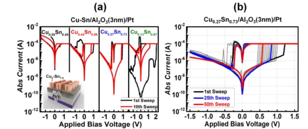
Figure 1.(a) Bipolar switching of CuSn-based device with different Cu and Sn concentrations. The black line displays the forming process (first cycle), and the red line represents the 10th cycle. Inset figure shows CuSn-based CBRAM. (b) Bipolar switching curves of Cu0.27Sn0.73/Al2O3/Pt for 50 cycles.
2
Figure 2.(a) Schematic view of CuSn/Lu- or/Dy-based CBRAM. Interfacial reaction observed by XPS at: (c) Dy/Al2O3interface, and;
(d) Lu/Al2O3interface.
Figure 3.C-AFM mapping images of Al2O3layer of devices with the Dy(top left) and Lu (bottom left) buffer layers and current profile along
removal rate was ∼0.95 nm/scan, providing sub-nanometer depth resolution.
2.3. Electrical & chemical characteristics
Current–voltage (I–V) measurements of the fabricated devi-ces were performed at room temperature using a semi-conductor characterization analyzer (Agilent B1500A). To obtain first-sweep (forming) RS, a positive voltage was applied to the modified electrode (CuSn), and the bottom Pt electrode was grounded. Furthermore, a waveform generator/ fast measurement unit (WGFMU) was used to measure the endurance of the device.
Analysis of the CuSn composition was performed by inductively coupled plasma optical spectrometry (Perki-nElmer Optima 8300). It included the assessment of atomic percentage(at.%) of the Cu–Sn alloy in four different com-positions. The chemical configuration at the Dy/Al2O3 or Lu/Al2O3 interface was confirmed by angle-resolved XPS (K-alpha).
3. Results and discussion
The CuSn alloy was used as the top electrode to control the amount of copper diffusion into the RS layer (Al2O3). Initi-ally, we investigated the effect of different compositions of
Cux–Sn1–x alloy(0.13<x<0.55) on the RS performance, as shown infigure1(a). The typical I–V relationships of the
Cux–Sn1–x/Al2O3/Pt/devices with an external current com-pliance of 100μA were measured to confirm the RS perfor-mance of the Cux–Sn1–x (0.13<x<0.55) alloy-based CBRAM devices. The optimal device was found to have a composition of Cu0.27–Sn0.73, which was sustained for more than 50 cycles of DC endurance, as shown infigure1(b), to
effectively control Cu diffusion and improve the RS perfor-mance of the device.
We inserted a high-density lanthanide metal (Dy: 8.55 g cm−3or Lu: 9.84 g cm−3) as a buffer layer between the Cu–Sn active electrode and Al2O3 layer, as shown in figure 2(a). Unlike previously reported metal buffer layers
[23, 25, 26], the lanthanide metal buffer layer has a high
density to control the penetration of Cu. Also, owing to the low electronegative potential of these metals, a significant interfacial oxide layer can be formed between the active electrode and the RS layer, which could act as an oxygen scavenger. The effect of the Dy or Lu metal buffer layer was investigated using XPS to identify the reaction of the lan-thanide metals at the interface with the Al2O3 layer. Figures2(b), (c) depict the binding energy of the core element
(Lu–O, Dy–O, Al–O, OH) in the O1s peak at the Dy/Al2O3 or Lu/Al2O3interface.
The O 1-s spectra at the interfaces of the devices are deconvoluted into three peaks. The lower binding energies of
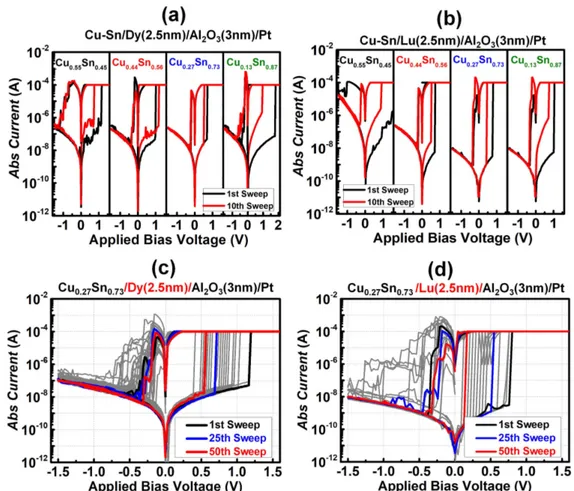
Figure 4.Bipolar switching curves of devices with different compositions of CuSn and a Dy(2.5 nm) buffer layer and (b) Lu (2.5 nm) buffer layer. Bipolar switching curves of(c) Cu0.27Sn0.73/Dy/Al2O3/Pt for 50 sweeps, and (d) Pt/Cu0.27Sn0.73/Lu/Al2O3/Pt for 50 sweeps.
4
529.2 eV, 529.4 eV, and 531.1 eV belong to Dy–O, Lu–O and Al–O respectively, and 532.2 eV of binding energy is shown for oxygen vacancies in the Al2O3layer. The percentage of the oxidation is slightly high in Dy–O compared to Lu–O, due to the low electronegativity of dysprosium [27]. The
oxida-tion of the buffer layers at the Dy//Al2O3 or Lu/Al2O3 interface was determined by the absorption of oxygen from Al2O3: the stronger the interfacial reaction between Lu or Dy and Al2O3, the greater the number of oxygen vacancies cre-ated on the Al2O3layer. In the oxygen vacancies, the CF grew vertically along the direction of oxygen deficiency and a relatively thin CF was formed on the Al2O3layer due to the Lu buffer layer[28,29]. Further, the C-AFM measurements
confirmed the controlled growth of the CFs in the devices. C-AFM is one of the most effective approaches to investigate internalfilament formation in a solid electrolyte [30–32]. In
the C-AFM measurements, a current amplification module and cantilever for contact-mode operation were used to measure the amplified current between the substrate and the cantilever.
A schematic sketch of the process flow of the C-AFM sampling is shown infigure S1 and is available online atstacks.
iop.org/NANO/29/385207/mmedia (supporting information).
Figure 3 shows the current mapping image obtained from C-AFM(left part) of the Al2O3layer of devices with the Dy and Lu buffer layers and the corresponding current (right part) profiles of the CFs. The bright region in the C-AFM image
denotes the filament area in the Al2O3 layer. It is the result found in the local region of the Lu buffer layer/Al2O3interface. The left part offigure3shows the current profile of the filament along the x-axis. The diameters of thefilament in the Dy and Lu buffer layer-based devices were different, but the maximum currentsflowing through the CF were the same (∼120 nA). We verified that a thin CF (from 10 nm to 40 nm) could be formed by inserting a Dy or Lu buffer layer. Figures4(a), (b) shows the
I–V curves of a 2.5 nm thick metal (Dy or Lu) buffer layer-based CBRAM device for different compositions of CuSn in the modified active electrode.
All the devices showed an on/off ratio improvement and reduced deterioration, as evidenced by the black(first sweep) and the red (10th sweep) lines. The electrical characteristics such as the on/off ratios and operating voltages were different for different compositions of CuSn; we confirmed that the device with the composition Cu0.27–Sn0.73 had a relatively uniform resistance distribution and showed stable operation. Figures 4(c), (d) show the DC sweeping of the optimized
Cu0.27–Sn0.73/Lu CBRAM device for 50 successive cycles. The on/off ratio of the Lu buffer layer device (106) was one order higher than that of the Dy buffer layer device (105), which could be ascribed to the relatively fewer oxygen vacancies in the Lu buffer device, forming a thinner CF due to the low penetration of Cu ions [33, 34]. In addition, we
compared the performance of the Cu0.27–Sn0.73devices with and without the buffer layers in terms of variation(cumulative
Figure 5.Cumulative probability of:(a) SET voltage and RESET voltage, and; (b) resistance states (LRS/HRS) of each device with and without the Dy or Lu metal buffer layer.(c) AC endurance test of HRS/LRS plotted as a function of the number of cycles for Dy and Lu buffer-based devices.(d) Retention test of HRS/LRS for Dy and Lu buffer-based devices at 85 °C.
probability) in SET/RESET voltages, resistance states, AC endurance, and long-term retention at 85°C. Figure 5(a)
shows the statistical distributions of the SET/RESET voltage obtained from cyclic curves for the Cu0.27–Sn0.73device with and without the Dy or Lu metal layer. The statistical approach was used to calculate the coefficient of variation (Cv) [35–37] for the average operating voltage of the devices with and without the buffer layer. Devices with Dy and Lu showed a smaller Cv value(SET/RESET: 30.8%/15.6% without buf-fer, 11.6%/9.5% for Dy buffer, 9.8%/9.2% for Lu buffer) and low operating voltages. The lanthanide buffer layer-based devices showed more uniform operating voltages due to the formation of relatively thin Cufilaments. Figure 5(b)
repre-sents the cumulative probability of the low resistance state (LRS)/HRS distribution of the Cu0.27–Sn0.73-based CBRAM devices with and without the Dy or Lu buffer layer. The Cvof the HRS for the devices decreased from 51.5% to 30.8% with the Dy buffer layer, and to 11.9% with the Lu metal layer. These data demonstrated the improvement in resistance uni-formity and on/off ratio (105–106). From the cumulative probability results, it could be verified that the Lu buffer layer interferes with the Cu-ion injection from the CuSn active electrode and that a thin CF contributed to the improvement in switching performance by controlling the oxygen defects at the interface. The Dy and Lu buffer layers enhanced not only the RS characteristics but also the reliability of the
CuSn-based CBRAM devices. AC endurance and retention were also analyzed to assess the operational reliability char-acteristics of the devices.
Figure5(c) shows the AC endurance of all three different
devices, obtained by applying AC pulses using a WGFMU. The applied pulse condition involves a SET pulse (1.7 V/ 10μs), read pulse (0.05 V/10 μs), and RESET pulse (−1.7 V/10 μs). The AC endurance performance of the Dy or Lu buffer layer-based devices was very stable up to 104 cycles. We believe that stable endurance in the Dy and Lu buffer layers devices is due to the formation/dissolution of tiny CFs under a uniform electric field, where the local electricfield strength is high compared to the randomly dis-tributed and thick CFs [34]. Moreover, we evaluated the
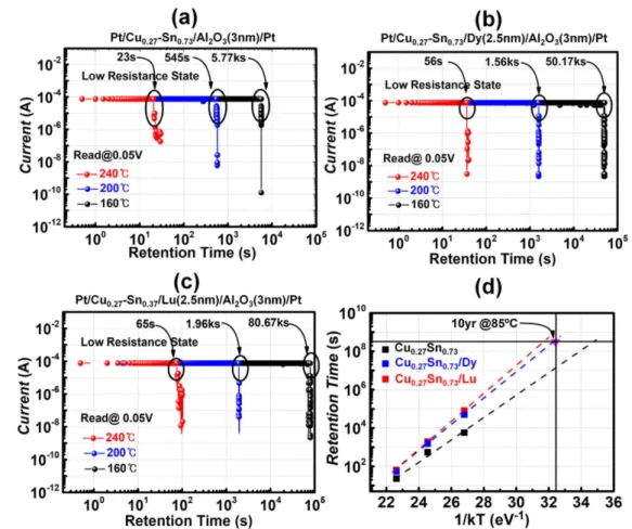
retention properties of the CuSn-based devices with lantha-nide metal buffer layers at a temperature of 85°C, as shown in figure 5(d); the results showed that the properties were
retained without significant corrosion for 104s. Also, LRS retention was evaluated to verify the robustness of the Cu– Sn/Lu or Dy buffer at high temperatures.
The ON state retention failure time at three different high temperatures (160 °C, 200 °C, and 240 °C) is shown in figures 6(a)–(c). The measurement revealed that the devices
with a Lu/Dy metal buffer layer were more stable than those without a buffer layer. This enhancement in retention could be explained as follows: when metal electrodes with two
Figure 6.(a)–(c) LRS retention test of Cu0.27–Sn0.73device with or without the Dy or Lu buffer layer at 160°C, 200 °C, and 240 °C.
(d) Mean time to failure of the Cu0.27–Sn0.73device with and without the Dy or Lu buffer layer.
6
effectively control the RS performance of CBRAM devices.
4. Conclusion
In this work, we demonstrated a way to control the overgrowth of CFs in the RS layer of CBRAM devices by combining a modified active electrode with a Lu or Dy metal buffer layer. At the optimal combination of Cu0.27Sn0.73/Lu or Dy (2.5 nm), the device showed highly stable RS characteristics, such as a high on/off ratio (106for Lu-based devices and 105 for Dy-based devices) with a long AC pulse endurance of about 10 000 cycles, low average operating SET (0.7 V) and RESET (−0.3 V) voltages, a good balance of HRS/LRS, and good retention up to 10 years. In addition, the Cu-filament formation is understood by the C-AFM. The improvements in the CuSn alloy along with the Lu/Dy buffer layer based RS memory suggests tha the new approach to improve the CBRAM devices for future non-volatile memories.
Acknowledgments
This research work was supported by the Basic Science Research Program through the National Research Foundation of Korea(NRF) grant funded by the Korean Government (MEST) (NRF-2017R1A2A2A05022574, 2015M3A7B7045496). ORCID iDs
Sanghun Jeon https://orcid.org/0000-0002-0414-9625
References
[1] Waser R and Aono M 2007 Nanoionics-based resistive switching memories Nat. Mater.6 833–40
[2] Sawa A et al 2008 Resistive switching in transition metal oxides Mater. Today11 28–36
[3] Terabe K, Hasegawa T, Nakayama T and Aono M 2005 Quantized conductance CBRAM Nature433 47–50 [4] Vishwanath S K and Kim J 2016 Resistive switching
characteristics of all-solution-based Ag/TiO2/Mo-doped
mechanisms, and performance Mater. Sci. Eng. R83 1–59 [10] Zhao X et al 2016 Forming-free electrochemical metallization
resistive memory devices based on nanoporous TiOxNythin
film J. Alloys Compd.656 612–7
[11] Jung S, Kong J, Song S, Lee K, Lee T, Hwang H and Jeon S 2010 Resistive switching characteristics of solution processed transparent TiOxfor nonvolatile memory
application J. Electrochem. Soc.157 H1042
[12] Tsuruoka T, Valov I, Tappertzhofen S, van den Hurk J, Hasegawa T, Waser R and Aono M 2015 Redox reactions at Cu,Ag/Ta2O5interfaces and the effects of Ta2O5film
density on the forming process in atomic switch structures Adv. Funct. Mater.25 6381
[13] You B K et al 2016 Reliable memristive switching memory devices enabled by densely packed silver nanocone arrays as electric-field concentrators ACS Nano10 9478–88
[14] Sun Y, Song C, Yin J, Chen X, Wan Q, Zeng F and Pan F 2017 Guiding the growth of a conductivefilament by
nanoindentation to improve resistive switching ACS Appl. Mater. Interfaces9 34064–70
[15] Shin K Y et al 2016 Controllable formation of nanofilaments in resistive memories via tip-enhanced electricfields Adv. Electron. Mater.2 1600233 (1–8)
[16] Mehdi S et al 2014 The effects of process variation on the parametric model of the static impedance behavior of programmable metallization cell(PMC) MRS Proc. 1692 (San Francisco, CA, USA)
[17] Mehdi S et al 2016 Carrier mobility extraction method in ChGs in the UV light exposure Micro Nano Lett.11 762 [18] Saremi M et al 2016 A physical-based simulation for the
dynamic behavior of photodoping mechanism in the chalcogenide materials used in the lateral programmable metallization cells Solid State Ionic290 1–5
[19] Vishwanath S K et al 2018 Enhancement of resistive switching properties in Al2O3bilayer-based atomic switches:
multilevel resistive switching Nanotechnology29 235202 [20] Lee M J et al 2011 A fast, high-endurance and scalable
non-volatile memory device made from asymmetric
Ta2O5-x/TaO2-xbilayer structures Nat. Mater.10 625–30
[21] Xiao N et al 2017 Resistive random access memory cells with a bilayer TiO2/SiOXinsulating stack for simultaneous
filamentary and distributed resistive switching Adv. Funct. Mater.27 1700384 (1–13)
[22] Woo H et al 2018 Resistive switching characteristics of a modified active electrode and Ti buffer layer in CuSe-based atomic switch J. Alloys Compd.753 551–7
[23] Rahaman S Z, Lin Y D, Lee H Y, Chen Y S, Chen P S, Chen W S, Hsu C H, Tsai K H, Tsai M J and Wang P H 2017 The role of Ti buffer layer thickness on the resistive switching properties of hafnium oxide-based resistive switching memories Langmuir33 4656–65
[24] Cho D-Y et al 2017 Interfacial metal−oxide interactions in resistive switching memories ACS Appl. Mater. Interfaces9
19287–95
[25] Jiang H et al 2016 Sub-10 nm Ta channel responsible for superior performance of a HfO2memristor Sci. Rep.6 28525
[26] Privitera S et al 2013 Study of the conductive filament in HfO2
resistive switching memory devices Microelectron. Eng.109
75–8
[27] Jeon S et al 2003 Effect of hygroscopic nature of the electrical characteristics of lanthanide oxides(Pr2O3, Sm2O3, Gd2O3
and Dy2O3) J. Appl. Phys.93 6393–6369
[28] Yang Y et al 2014 Electrochemical dynamics of nanoscale metallic inclusions in dielectrics Nat. Commun.5 4232 [29] Ju J H, Jang S K, Son H, Park J H and Lee S 2017 High
performance bi-layer atomic switching devices Nanoscale
9 8379
[30] Celano U et al 2013 Filament observation in metal-oxide resistive switching devices Appl. Phys. Lett.102 121602 [31] Celano U et al 2013 Switching mechanism and reverse
engineering of low-power Cu-based resistive switching devices Nanoscale5 11187–92
[32] Zhao Y D, Huang P, Guo Z H, Lun Z Y, Gao B, Liu X Y and Kang J 2016 Atomic Monte-Carlo simulation for CBRAM with variousfilament geometries Simul. Semicond. Processes Devices 153–6 21.6.1–21.6.4
[33] Zhao X et al 2017 Confining cation injection to enhance CBRAM performance by nanopore graphene layer Small13 1603948
[34] Mondal S, Chueh C-H and Pan T-M 2014 Current conduction and resistive switching characteristics of Sm2O3and Lu2O3
thinfilms for low-power flexible memory applications J. Appl. Phys.115 014501
[35] Wang G et al 2015 Impact of program/erase operation on the performances of oxide-based resistive switching memory Nanoscale Res. Lett.10 39
[36] Yoon J H, Song S J, Yoo I-H, Seok J Y, Yoon K J, Kwon D E, Park T H and Hwang C S 2014 Highly uniform,
electroforming-free, and self-rectifying resistive memory in the Pt/Ta2O5/HfO2−x/TiN structure Adv. Funct. Mater.24 5086–95
[37] Gao S et al 2018 Improving unipolar resistive switching uniformity with cone-shaped conductingfilaments and its logic-in-memory application ACS Appl. Mater. Interfaces10
6453–62
[38] Attarimashalkoubeh B, Prakash A, Lee S, Song J, Woo J, Misha S H, Tamanna N and Hwang H 2014 Effect of Ti buffer layer on retention and electrical characteristics of Cu-based conductive-bridge random access memory(CBRAM) ECS Solid State Letters3 P120–2
[39] Yang Y and Lu W 2013 Nanoscale resistive switching devices: mechanisms and modelling Nanoscale5 10076–92 [40] Aga F G, Woo J, Lee S, Song J, Park J, Lim S, Sung C and
Hwang H 2016 Retention modelling for the ultra-thin density of Cu-based conductive bridge random access memory(CBRAM) AIP Adv.6 025203
8