P1-90 / C. H. Yun
IMID 2009 DIGEST •
Abstract
We present multilayer transparent electrodes (MTEs) that resulted in organic light-emitting diodes (OLEDs) with the 90 % higher forward luminous efficiency and 30% higher external quantum efficiency (EQE) than conventional ITO based devices respectively. Optimization method of such MTE structure is investigated in consideration of both injection and optical structure.
1. Introduction
Indium tin oxide (ITO) films have been a popular choice for transparent electrodes in organic light-emitting diodes (OLEDs) for several decades. However, the potential shortage of indium supply has made many researchers investigate new types of transparent electrodes [1]. Among many alternatives to ITO films, a special attention has been paid to the dielectric/ metal/ dielectric (DMD) multilayer system, because it can have a high sheet conductance and transparency comparable to those of conventional ITO films [2] and because its injection property can be varied by choosing the right dielectric material interfacing organic semiconductors. Recently, we have demonstrated that ZnS/Ag/WO3 (ZAW) electrodes can
lead to a high-performance flexible OLEDs with the mechanical flexibility that is far superior to those based on ITO electrodes [3]. In spite of such recent developments, there has been no study devoted to the optimization of DMD structures which requires the overall account of the optical structure and injection behavior.
In this study, we investigate how the luminous efficiency of OLEDs varies depending on the structure of ZnS/Ag/WO3 electrodes in consideration of both
optical and electrical properties. And then, the optimization method is proposed by which the luminous efficiencies as well as power efficiencies can be maximized.
2. Experimental
Multilayer transparent electrodes (MTEs) consisting of ZnS (x nm; varied), Ag (20nm), and WO3 (y nm; varied) were prepared on a glass substrate
planarized with polymeric films (SU-8, Kayaku Microchem) by a thermal evaporation. 20nm-thick Ag films were shown to provide a sheet conductance as small as 6 Ω/sq. The ZnS layer on the glass substrate is used to enhance the optical transparency of MTEs in this study, and WO3 is used for hole-injection to
organic semiconductor as well as for enhancement of transparency. OLEDs were in normal bottom-emission geometry, and were based on N,N'-Bis(naphthalen-1-yl)-N,N'-bis(phenyl)-benzidine (NPB) as a hole transporting layer, Tris(8-hydroxy-quinolinato) aluminium (Alq3) as an emitting and electron transporting layer, and LiF/Al as a cathode. OLEDs based on a conventional ITO glass were also made in the same batch for comparison. To confirm the influence of ZAW electrode in OLEDs, the thickness of NPB and Alq3 were fixed at 50 nm, respectively.
The measurement for OLEDs was done in a nitrogen-filled glove box. EL spectra were obtained with a fiber optic spectrometer (EPP2000, StellarNet). Current-voltage (J-V) and luminance-voltage (L-V) characteristics were recorded with a source-measure unit (Keithley 2400) and a calibrated photodiode (FDS100, Thorlab).
In optimization method, some of the optical constants used in the simulation were measured by the spectral ellipsometry and the others were borrowed from the commercial software (The Essential Macleod, Thin Film Center, Inc.) for thin film optics. The program was also used to analyze the overall optical properties of OLEDs under study.
High efficiency organic light emitting-diodes (OLEDs)
using multilayer transparent electrodes
Changhun Yun, Hyunsu Cho, and Seunghyup Yoo*
1Dept. of Electrical Engineering, KAIST, Daejeon, Republic of Korea
P1-90 / C. H. Yun
• IMID 2009 DIGEST
3. Results and discussion
Different from the ITO-based device, OLEDs with ZnS/Ag/WO3 (ZAW) as a transparent electrode can
form a micro-cavity structure between the highly reflective cathode (Al) and the ZAW anode depending on the transmission of ZAW electrodes. Generally, the intensity of an emitted light from the resonator can be described by following equation, assuming the organic layers can be regarded as a single layer [4]:
I
(
λ θ,)
= fFP ⋅fTI ⋅IO(
λ θ,)
(1) where(
)
2 2 1 4 2 FP ZA W A l ZA W A l ZA W f T R R R R sin ∆φ = ⎛ ⎞ − + ⎜ ⎟ ⎝ ⎠ (2),(
)
1 4 2 TI A l org o org,EM L A l A l f R n z cos R cos φ π θ λ = + ⎛ ⎞ ⎜ ⎟ + − + ⎜ ⎟ ⎝ ⎠ (3), and(
)
Al ZAW 4 i i org,i i n d cos π θ ∆φ φ φ λ = − − +∑
(4).In the above equations, fFP, fTI and I0(λ,θ)
correspond to the Fabry-Perot multiple beam interference factor, a two-beam interference factor, and an electro-luminance spectrum of emissive layer at a wavelength λ and an emission angle θ, respectively. As one can see in equations (2) and (3), fFP and fTI terms can be affected by the transmittance
and the reflectance of ZAW electrode, related to the thickness of both ZnS and WO3.
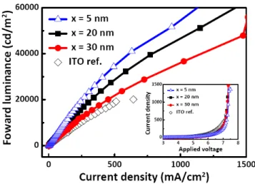
Figure 1 shows the L-J, and J-V (inset in Fig. 1) characteristics of OLEDs with ZAW electrodes, for different thicknesses of WO3 layers in comparison to
those with conventional ITO electrodes. (Here L was measured at θ= 0.)
In case of luminous efficiency, which can be measured from the slopes of L-J curves in Fig.1, ZAW-based OLEDs clearly outperform ITO-based OLEDs, in the normal direction to substrates. It is noted that the thinner WO3 layer shows the higher
device efficiency even though ZAW electrodes with the thicker WO3 layer are more transparent. As fTI is
common for all the devices, it is considered that the higher efficiency comes from the better match between the peaks of fFP and Alq3 EL spectrum.
Fig. 1. OLED characteristics with the structure of glass/ X/ NPB(50nm)/ Alq3(50nm)/ LiF:Al. X= ITO or ZnS(40nm)/ Ag(20nm)/ WO3 (5nm, 20nm, 30nm):
Forward luminance vs current density curve and current density vs applied voltage curve (inset)
As the thickness of WO3 increases, the phase term
upon reflection at ZAW electrodes will vary to accommodate the increased thickness of WO3 layers,
resulting in the net red-shift of the resonance wavelength in micro-cavity terms.
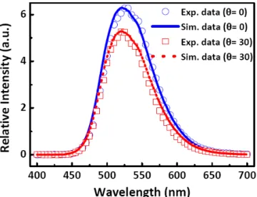
Fig.2 is the intensity variation of OLEDs with ZnS (30nm)/Ag (20nm)/WO3 (5nm) electrode as a function
of emission angle θ. Normally, the light output of ITO-based OLEDs is Lambertian, where the intensity decreases following cosθ as θ increases. (See the dotted line in Fig. 2.) In ZAW-based OLEDs, however, the intensity drops slightly quicker than the ideal Lambertian curve.
Fig. 2. Intensity distribution over oblique angles: In y-axis, the intensities are normalized by the intensity of the forward direction. (θ= 0)
P1-90 / C. H. Yun
IMID 2009 DIGEST • Fig. 3. Electro-luminance spectrum of OLEDs based on
glass/ ZnS(30nm)/ Ag(20nm)/ WO3(5nm)/ NPB(50nm)/
Alq3 (50nm)/ LiF:Al. : The solid and dotted lines correspond to the simulation results by using Equation (1).
It is because the resonance wavelength goes shorter and thus the resonance mismatch with respect to the emission spectrum grows as θ increases. This behavior is confirmed in Fig.3 showing the slight blue-shift of EL spectrum peak at an oblique angle. Experimental data were also shown to match well with the modeling results.
Fig. 4. OLED characteristics with the structure of glass/ Y/ NPB(50nm)/ Alq3(50nm)/ LiF:Al. Y= ITO or ZnS(30nm, 45nm, 60nm)/ Ag(20nm)/ WO3 (5nm): Forward luminance vs current density curve and current density vs applied voltage curve (inset)
Fig.4 presents L-J and J-V (inset in Fig. 4) characteristics of OLEDs with different thicknesses of ZnS layers. In this case, the OLED with 60 nm-thick ZnS showed the best performance, although the relative difference was smaller than the previous case. It is noted that the ZAW electrode with 60nm-thick ZnS layer is the least transparent among the three samples compared. Considering the major interface of reflection within ZAW electrode is Ag/WO3 interface, the variation of ZnS thickness would not affect the cavity length much. However, a special attention still needs to be paid because it influences the overall transmittance and the reflectance of ZAW electrodes, which affect the Fabry-Perot factor.
4. Summary
OLED devices using ZnS/Ag/WO3 (ZAW) multilayer
transparent electrode (MTE) exhibit the luminous efficiency and power efficiency that are far superior to those based on any other alternatives to ITO films and to those with ITO films themselves. These MTEs can be easily prepared using a thermal evaporation that is widely adopted in the OLED industry and is mild enough to be used in top-emitting geometry without concerns on plasma-induced damage.
In this work, we investigated the overall optical structure of ZAW electrode in a full micro-cavity geometry, which will lay the foundation for optimization of OLEDs with MTEs in general.
Acknowledgement
This work was supported by ERC program of the Korea Science and Engineering Foundation (KOSEF) grant funded by the Korea Ministry of Education, Science and Technology (MEST) (No. R11-2007-045-03002-0) and by the Human Resource Training Project for Strategic Technology by the Korea Industrial Technology Foundation (KOTEF).
5. References
1. A. Chipman, Nature 449 (7159), 131 (2007)
2. X. J. Liu, X. Cai, J. S. Qiao, H. F. Mao and N. Jiang, Thin Solid Films 441, 200-206, (2003).
3. H. Cho, C. Yun, J.-W. Park and S. Yoo, Org. electron. 10, p.1163 (2009)
4. B. Jung and C. Hwangbo, J. Kor. Phys. Soc. 48, p.1281 (2006).