P1-14 / D. W. Kim
• IMID 2009 DIGEST
Abstract
We have examined the silicon nitride (SiNx) as gate
insulator with the ammonia (NH3) plamsa treatment
for the soluble derivatives of polythiophene as p-type channel materials of organic thin film transistors (OTFTs). Fabrications of the jetting-processed OTFTs with SiNx as gate insulator by NH3 plasma treatment
can be similar to performance of OTFTs with silicon dioxide (SiO2) insulator.
1. Introduction
Recently, Organic thin-film transistors (OTFTs) have been researched for many applications such as sensors, smart cards, identification tags, and the display devices including flexible displays [1]. High performance OTFTs has been mostly achieved in top-contact device configuration rather than bottom-contact device configuration [2, 3]. However, top-contact device configuration is incompatible with lithography process due to the sensitivity of organic semiconductors to ultraviolet, electron beam, and chemical wet processes. This limitation makes top-contact configuration undesirable for manufacturing [4]. Bottom-contact configuration source–drain (S–D) electrodes can be easily fabricated by lithography process and thus are much more promising than top-contact configuration for large scale integration and manufacture of OTFTs. In this paper, we have investigated the soluble OTFT through the NH3 plasma Treatment for the SiNx as a gate insulator for mass-productions. For enhancement of performance OTFTs, The SiNx is improved by optimized NH3 plasma treatment [5].
2. Experimental Procedure
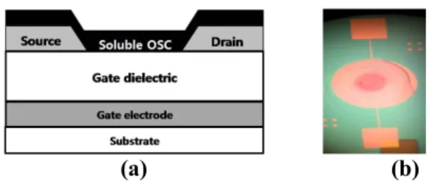
To compare effects of the NH3 plasma treatment on SiNx surface, we fabricated bottom contact OTFT devices with circle type source-drain electrode by solution jetting process as shown in Fig.1.
(a) (b)
Figure 1. Configurations of (a) bottom-gate & bottom contact structure and (b) circle type source-drain electrode with SiNx as gate insulator.
The thermally SiO2 wafer with the total thickness about 3000 Å was prepared. The OTFTs devices are fabricated for a bottom contact configuration on a degenerately doped n+ silicon wafer used as a gate electrode. Also, Chrome (Cr) metal layer as gate electrode was deposited by a sputter with the thickness of 300 Å on galss substrate.SiNx films were deposited in a parallel-plate plasma enhanced chemical vapor deposition (PECVD) reactor operating at an excitation frequency of 13.56 MHz. The process pressure was maintained at 800 mTorr, the substrate temperature was 300 °C, and the rf power was 300 W. The nitrogen (N2), ammonia (NH3) and silane (SiH4) gas flow rate ratio are 8:1:2. After SiNx film deposition with the thickness about 2000 Å, it is annealing by the Rapid Thermal Annealing (RTA) at 300 °C. SiNx films were treated by the nitrous oxide (N2O) / NH3 plasma. The N2O / NH3 plasma were generated under the conditions of the working pressure 250 mTorr, the substrate temperature 300 °C, the RF power 50 W and the gas flow rate 100 sccm for 12 min, respectivly. For the formation of circle type source-drain electrodes, Au metal layer was deposited by a thermal evaporation with thickness of 300 Å, and patterned by photo-lithography and wet chemical etching processes; the channel width (W) and length
Fabrication of soluble organic thin film transistor with ammonia (NH
3)
plasma treatment
Dongwoo Kim, Doohyun Kim, Keonsoo Kim, Hyoungjin Kim, Hong Choi
Donghyeok Lee and Munpyo Hong*
Dept. of Display and Semiconductor Physics, Korea University, Chungnam, KOREA
P1-14 / D. W. Kim
IMID 2009 DIGEST • (L) were defined as 3000 μm and 5 μm, respectively.
The Poly(3-hexylthiophene) (P3HT) precursor was dissolved in tetralin solvent. This solvent was chosen over chloroform due to its slower evaporation rate, making it more suitable for our home-made jetting system. After jetting the OSC on circle type Au electrodes, the device samples were annealed at 150 °C for 30 min in N2. The performances of OTFTs were measured by semiconductor parameter analyzer (HP4156C) in dark spaced probe station at room temperature.
3. Results and discussion
The field-effect mobility at VD=VG was calculated by
where μfe is the field-effect carrier mobility, VT is the threshold voltage, W is the channel width, L is the channel length, Ci is the capacitance per unit area.
20 15 10 5 0 -5 -10 -15 -20 -25 -30 -35 -40 -13 -12 -11 -10 -9 -8 -7 -6 -5 -4 Transfer Curve Drain-Source voltage (VD=-10V)
SiNx with NH3 plasma treatment SiNx with NO2 plasma treatment SiNx without any plasma treatment
SiO2 without any plasma treatment
Gate Voltage(V)
Log Drain Current
(A)
Figure 2. The electric characteristics of OTFTs with various films ID-VG, (W/L = 3000 μm / 5 μm)
Figure 2 illustrates the transfer characteristics of a typical P3HT OTFT on SiO2, SiNx and SiNx with N2O / NH3 plasma treatment. In SiO2 insulator without any plasma treatment, the field-effect mobility of OTFTs with jetting process is about 0.002 cm2V-1s-1. On the
other hand, the performance OTFTs using the SiNx as gate dielectric without any plasma treatment drive as the field effect mobility (μfe) of 0.002 cm2V-1s-1, the threshold voltage (VT) of -22.0 V, the sub-threshold slope (S-S) of 0.74 V/dec and the on-off currents ratio (Ion/Ioff) of 107. However, the result by N2O plasma treatment is inferior to that by bare SiNx to the effect of damage of N2O plasma.
In our experiment, the SiNx with NH3 plasma treatment drive best results as μfe of 0.003 cm2V-1s-1,
the VT of -17.0 V, the S-S of 0.53 V/dec and the Ion/Ioff of 5*106, due to the effect of nitrogen-rich nitride.
Table I. Summary of the electrical parameters for the OTFTs. μfe is the room temperature field-effect mobility, S is the sub-threshold swing, VT is the threshold voltage.
4. Summary
P3HT OTFTs on SiNx (i.e., nitrogen-rich nitride) gate dielectric have performance comparable to that of OTFTs fabricated on thermal SiO2 gate dielectric (average mobility of 0.002 cm2/Vs and on/off ratio of over 107). Consequently, OTFTs on SiNx using NH
3 plasma treatment is similar to performance of OTFTs with SiO2 insulator. Also, Investigation of lower temperature SiNx using various plasma treatments as gate dielectric for Soluble OTFTs is currently in progress.
Acknowledgements
This research was supported by a grant (F0004012-2009-32) from information display R&D Center, one of Knowledge Economy Frontier R&D of Korean Government and Korea University Grant.
5. References
[1] C. D. Dimitrakopoulos, P. R. L. Malenfantols, Adv. Mater., 14. 99 (2004)
[2] G.R. Dholakia, M. Meyyappan, A. Facchetti, T.J. Marks, Nano Lett. 6 (2006) 2447.
[3] I. Kymissis, C.D. Dimitrakopoulos, S.
Purushothaman, IEEE Trans.Electron Devices 48 (2001) 1060.
[4] M.M. Ling, Z. Bao, Chem. Mater. 16 (2004) 4824.
[5] F. M. Li, A. Nathan, Y. Wu and B. S. Ong, Appl. Phys. Lett. 90, 133514 (2007) Gate Insulator (cmμ2fe V-1 s-1 ) S (V/dec) V(V) T Ion/Ioff (a) SiOx 0.002 0.98 -14.0 5*107 (b) SiNx 0.002 0.74 -22.0 107 (c) SiNx with N2O plasma treatment 0.001 1.30 -21.0 105 (d) SiNx with NH3 plasma treatment 0.003 0.53 -17.0 5*106 ) 1 ( ) ( 2 2 ,sat i G T D C V V L W I ⎟ − ⎠ ⎞ ⎜ ⎝ ⎛ =