32-1 / S.-H. K. Park
IMID 2009 DIGEST •
Abstract
We have investigated the effect of the device structure on the performance of polycrystalline ZnO TFT and amorphous AZTO TFT with top gate and bottom gate structure. While the mobility of both TFTs showed relatively similar value in a top and bottom gate structure, bias stability was quite different depending on the device structure. Top gate TFT showed much less Vth shift under positive bias stress compared to that of bottom gate TFT. We attributed this different behavior to the defects formation on the gate insulator induced by energetic bombardment during the active layer deposition in a bottom gate TFT. We suggest the top gate oxide TFT would show more stable behavior under the Vgs bias.
1. Introduction
During last a couple of years, there was astonishing development in oxide TFTs. The needs for the oxide TFT have been mostly focused on the backplane of AM-Display including LCD, OLED, flexible display, and transparent display.1-4 Many
papers describing the fabrication and performance of oxide TFTs have been reported.5-7 High mobility,
uniformity, fairly good stability, and low cost process make oxide TFTs applied even to a large size AM displays.
There was a break-through in oxide TFT technology. 12” AM-OLED and 15” TFT-LCD driven by amorphous oxide TFT and AM-OLED driven by fully transparent ZnO TFT have been demonstrated in 2008. It seems that oxide TFT would be the best candidate of backplane for the next generation AM displays and the remained issues for the mass production of oxide TFT are the electrical and optical stability.
There are several issues in getting electrically high stable oxide TFT such as interface, gate insulator process, and oxide semiconductor. Here we investigated the effect of device structure on the
performance of oxide TFT particularly in terms of bias stability for the polycrystalline ZnO TFT and amorphous AZTO TFT.
2. Experimental
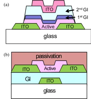
We fabricated bottom and top gate structured TFTs to investigate the effect of device structure on the oxide TFT characteristics as shown in the figure 1.
Figure 1. Schematic diagram of (a) top gate and (b) bottom gate structure of oxide TFT.
In the case of top gate structure, ITO was deposited on a glass substrate as a source/drain (S/D) in 150 nm thick. After patterning of ITO (S/D), ZnO and AZTO were deposited by means of PEALD and RF-magnetron sputtering, respectively. After thin alumina which plays a role of active protection layer (PL) as well as the first gate insulator (GI) was deposited by ALD, the active layer and PL were patterned by wet etching at once. The alumina (2nd gate insulator) was
Oxide TFT Structure Affecting the Device Performance
Sang-Hee Ko Park, Doo-Hee Cho, Chi-Sun Hwang, Minki Ryu, Shinhyuk Yang, Chunwon Byun, Sung Min Yoon, Woo-Seok Cheong,
and Kyoung Ik Cho
Transparent Display Team, ETRI, Daejeon 305-350, Korea Phone:82-42-860-6276, E-mail: [email protected]
Keywords: oxide TFT, ZnO, AZTO, device structure
1stGI
2ndGI
ITO Active ITO
ITO glass (a) glass passivation Active ITO ITO ITO GI (b)
32-1 / S.-H. K. Park
• IMID 2009 DIGEST
deposited by ALD, followed by S/D pad opening by wet etching of alumina. Sputtered ITO layer was used as gate electrode and patterned. In the case of bottom gate structure, ITO coated glass was used for the substrate. After patterning of ITO gate electrode by wet etching, gate insulator, alumina, was deposited by means of ALD, followed by gate electrode pad opening by wet etching of alumina. Sputtered ITO was used as S/D electrodes and patterned by wet process. In the case of ZnO TFT, ZnO and PL were patterned at once by wet etching process. In the case of AZTO TFT, however, AZTO film was patterned, followed by deposition of alumina by ALD to passivate AZTO bottom gate devices. We fabricated transparent AM-OLED which has top gate ZnO TFT array in a same way except the gate electrode. Sputtered Oxide/Ag/Oxide (OMO) layer with thickness of 100 nm was used as gate electrode and patterned. The low resistance of OMO layer enables us to minimize the IR drop of TFT array keeping its transparency. For the integration of OLED, ZnO TFT array was coated with transparent polymer dielectric material for the planarization. OLED anode, ITO, was deposited by sputter and patterned by wet process, followed by OLED bank process. The structure of OLED fabricated by vacuum thermal deposition was NPB/ DPVBI:BD/ LGET185/ LiF/ Al/ Ag. OLED encapsulation was carried out using cover glass with getter.
3. Results and discussion
There was no report which compares the device performance of bottom gate and top gate TFT with same active layer and gate insulator since controlling carrier amount in a semiconductor is very difficult for TFT to behave well in both structures. With use of alumina layer deposited by ALD for the formation of the interface between the active layer and gate insulator or active layer and passivation layer, we could obtain well behaved ZnO TFT and AZTO TFT in both structures. From our previous results, we figured out that the main issue in the device stability comes from the interface formation process and plasma damage free process during the interface formation is very important to get electrically stable oxide TFT. Therefore, in this paper we adopted plasma free interface formation process using alumina deposited by ALD with water oxygen source just to compare the device structure effect on the TFT characteristics.
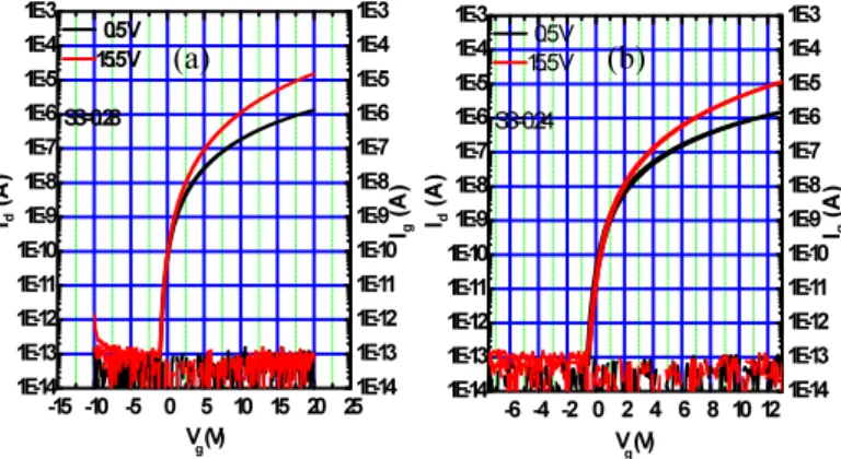
In the case of polycrystalline ZnO, film properties
of bottom layer which acts as a channel in a bottom gate and top layer which plays as a channel in a top gate would be different. As show in the figure 2, the mobility of bottom gate is 3.12 cm2/V.s, while that of
top gate is 4.63 cm2/V.s.
Figure 2. Transfer characteristics of ZnO-TFT in a (a) bottom gate with pristine alumina GI, (b) bottom and (b) top gate structure (W/L=40/20) for VDS varying
from 0.5 to 15.5V
Distinguishing difference between the transfer characteristics of these two devices were Vth. With alumina deposited by ALD at low temperature, we have to worry about the hydrogen incorporation from the gate insulator to the ZnO as well as the trap site on the surface.
Figure 3. Transfer characteristics of ZnO-TFT in a bottom gate (a) with annealed alumina GI, (b) with alumina deposited using ozone just for the interface (W/L=40/20) for VDS varying from 0.5 to 15.5V
To clarify these effects, we fabricated bottom gate device with alumina annealed at 300oC under vacuum
before deposition of ZnO and with alumina deposited with ozone precursor at 350oC. The Vth of these two
bottom gate ZnO TFT are almost similar to that of top gate ZnO TFT. -35 -30 -25 -20 -15 -10 -5 0 5 1E-14 1E-13 1E-12 1E-11 1E-10 1E-9 1E-8 1E-7 1E-6 1E-5 1E-4 1E-3 1E-14 1E-13 1E-12 1E-11 1E-10 1E-9 1E-8 1E-7 1E-6 1E-5 1E-4 1E-3 Id (A ) Vg (V) 0.5 V 15.5 V Ig (A ) (a) -15 -10 -5 0 5 10 15 20 25 1E-14 1E-13 1E-12 1E-11 1E-10 1E-9 1E-8 1E-7 1E-6 1E-5 1E-4 1E-3 1E-14 1E-13 1E-12 1E-11 1E-10 1E-9 1E-8 1E-7 1E-6 1E-5 1E-4 1E-3 Id (A ) Vg (V) 0.5 V 15.5 V Ig (A ) (b) -15 -10 -5 0 5 10 15 20 25 1E-14 1E-13 1E-12 1E-11 1E-10 1E-9 1E-8 1E-7 1E-6 1E-5 1E-4 1E-3 1E-14 1E-13 1E-12 1E-11 1E-10 1E-9 1E-8 1E-7 1E-6 1E-5 1E-4 1E-3 Id (A ) Vg (V) 0.5 V 15.5 V SS=0.28 Ig (A ) (a) -6 -4 -2 0 2 4 6 8 10 12 1E-14 1E-13 1E-12 1E-11 1E-10 1E-9 1E-8 1E-7 1E-6 1E-5 1E-4 1E-3 1E-14 1E-13 1E-12 1E-11 1E-10 1E-9 1E-8 1E-7 1E-6 1E-5 1E-4 1E-3 Id (A ) Vg (V) 0.5 V 15.5 V SS=0.24 Ig (A ) (b)
32-1 / S.-H. K. Park
IMID 2009 DIGEST •
Even though the characteristics of bottom and top gate ZnO TFT is not different significantly, the gate bias stabilities were very different and these results are almost similar to those of amorphous AZTO TFT. We fabricated bottom and top gate AZTO TFTs. Amorphous AZTO TFTs in a bottom and a top gate have similar mobility of 12 cm2/V.s. The gate bias
stability, however, was completely different and top gate AZTO TFT showed much smaller Vth shift under positive gate bias compared to that of bottom gate TFT as shown in figure 4.
Figure 4. Bias stability of AZTO TFT (Vg = 20 V) at RT in a (a) bottom gate structure and (b) top gate structure (W/L=40µm/20µm).
The bias stability of oxide TFT is quite dependent on the interface formation process and particularly sensitive to the plasma damage on the gate insulator during the deposition sequence of channel and gate dielectric layer. In a top gate, there would be no plasma damage on the gate insulator and rather we have to worry about the damage on the channel from the following process. Meanwhile, in the bottom gate structure, there is no way to get rid of plasma damage on the gate insulator during the active layer deposition as long as we have to use plasma process such as
sputtering and PEALD. This energetic bombardment on the gate dielectric during the initial channel deposition from plasma process directly affects device stability to result in poor bias stability. Therefore, it would be very important to minimize and to get rid of plasma damage on the gate insulator to get highly stable oxide TFT.
However, we also figured out that the instability induced during the active layer process is quite dependent on the cation composition of active layer. With special composition cation, we can get hysteresis free bottom gate device with high stability as will be reported in other session of this conference.
The other factor which should be considered in a bottom gate structure is the passivation layer process. The passivation process in a bottom gate affected exactly same way to the first gate insulator process in a top gate structure. Therefore, it is very important to adopt each passivation layer suitable for each active layer to get highly stable oxide TFT.
We have fabricated 2.9 inch 176 x 220 transparent AM-OLEDs with top gate AZTO-TFT and ZnO- TFT shown in figure 5.
Figure 5. Operating image of transparent AM-OLED driven by (a) top gate AZTO TFT and (b) top gate ZnO TFT.
4. Summary
We have investigated the effect of oxide TFT
structure on the device performance including bias stability. Contrary to the top gate structure which can
panel size 2.9” resolution 176 x 220 pixel pitch 230 x 215 µm2 -15 -10 -5 0 5 10 15 20 1E-14 1E-13 1E-12 1E-11 1E-10 1E-9 1E-8 1E-7 1E-6 1E-5 1E-4 1E-3 Id (A ) Vg (V) 0s 30s 100s 300s 1ks 3ks 7.2ks 10ks (a) -15 -10 -5 0 5 10 15 20 1E-14 1E-13 1E-12 1E-11 1E-10 1E-9 1E-8 1E-7 1E-6 1E-5 1E-4 1E-3 0.000 0.002 0.004 0.006 0.008 Id (A ) Vg (V) 0s 30s 100s 300s 1ks 3ks 10ks 30ks 36ks (b) (a) (b)
32-1 / S.-H. K. Park
• IMID 2009 DIGEST
be fabricated without induction of plasma damage on the gate insulator, bottom gate TFT cannot avoid energetic bombardment on the gate insulator during the active layer formation. This resulted in a big difference between the bias stability of the top and bottom gate TFT. We showed the device structure effect on the bias stability for the first time and this provides good methodology to get highly stable oxide TFT.
Acknowledgement
This work was supported by the IT R&D program of MKE, [2006-S079-04, Smart window with transparent electronic devices].
5. References
1. J. Lee et al. SID 08 DIGEST, p 625 (2008).
2. J. K. Jeong et al. SID 08 DIGEST, p 1 (2008).
3. C.S. Hwang et al. IMID 08 Proceeding (2008).
4. S.-H. K. Park et al, SID 06 DIGEST, p 25 (2006).
5. K. Nomura et al, Nature,432, p 488(2004).
6. J. K. Jeong et al. Appl. Phys. Lett., 91, p 113505, (2007).
7. M.-C. Sung et al, IMID 07 Proceeding, p 133 (2007).