P1-99 / J. Y. Cai
• IMID 2009 DIGEST
Abstract
The concept of a microplasma current switch for a device operated in a current mode like organic light-emitting diodes, which features matrix addressability and current switching, is presented as well as its architecture and operational principle. To verify the concept, we have fabricated a 100 mm × 100 mm microplasma current switch panel with a cell pitch of 1080 µm × 1080 µm. Moreover, the current-voltage measurements of the unit cell are performed for three different driving voltage amplitudes. They show the characteristic of an asymmetric floating double probe diagnosing plasmas.
1. Introduction
Microplasmas have been studied extensively on account of their useful properties and wide applications to electronic devices. A typical device employing microplasmas is a plasma display panel (PDP) where microplasma discharges are ignited to generate ultraviolet rays, causing phosphors to be excited and emit light. An array of discharge cells is normally fabricated in rows and columns between a pair of plates of glass, and the discharge cells are operated by matrix addressing without an extrinsic active element owing to their inherent memory [1-3].
Another device utilizing microplasmas is a plasma addressed liquid crystal display (PALCD) where discharge channels along the scan lines are formed as an extrinsic active element to achieve active matrix addressability. Taking advantage of plasma space potential, the discharge channels function as a switch to drive liquid crystal cells in a voltage mode [1, 4].
In general, amorphous silicon (a-Si) or polycrystalline silicon (poly-Si) thin film transistors (TFTs) are adopted as switching elements in active
matrix organic light-emitting diodes (AMOLEDs). Since organic light-emitting diodes (OLEDs) are operated in a current mode, AMOLEDs need at least two TFTs and one capacitor in each pixel. Furthermore, to compensate for the nonuniformity of poly-Si TFTs or the threshold voltage shift of a-Si TFTs, AMOLEDs require more than three transistors and one capacitor in each pixel, and hence have a complicated pixel circuit, structure, and fabrication process [5, 6].
In this study, we present a microplasma current switch (MPCS), where the intrinsic memory and conductivity of plasmas are utilized to achieve matrix addressability and current switching, as well as its current-voltage characteristic and analysis. The MPCS is applicable as an active element to a current-driven device like OLEDs, and it can be employed as a probe for diagnosing microplasmas as well.
2. Device Concept
The conceptual device architecture of MPCS-OLEDs is schematically illustrated in Fig. 1. It consists of front and rear plates holding a mixture of inert gases. The configuration of the rear plate is similar to that of a coplanar alternating current plasma display panel (AC-PDP) except for the address electrode location. Address and sustain electrodes are all placed on a rear glass substrate. The front plate includes a front glass substrate, OLED, insulation and cathode layers. While the anode electrode of the OLED is connected to a direct current (DC) power supply, its cathode electrode is “floating,” that is, it is not connected to the DC power supply. An insulation layer with an opening is formed on the floating cathode electrode. A cathode layer, which is connected
Microplasma Current Switch for OLED applicatio
ns
Jie Yu Cai
1, Myung-Min Kim
1, Cheol-Hee Moon
1, Sang-Youn Lee
2, and
Seungjun Yi
21Dept. of Display Eng., Hoseo Univ., Asan-Shi, Chungnam 336-795, Korea
2Dept. of Semiconductor/Display Eng., Hoseo Univ., Asan-Shi, Chungnam 336-795, Korea
Tel.:82-41-540-9655, E-mail: [email protected]
P1-99 / J. Y. Cai
IMID 2009 DIGEST • to the DC power supply, is formed apart from the
floating cathode electrode on the insulation layer. When plasmas are initiated by the sustain electrodes connected to an alternating current (AC) power supply, a current path is formed by the plasmas between the floating cathode electrode and cathode layer due to the plasma conductivity. As a result, current flows through the plasmas and then the OLED emits light. The conductive plasmas act as a current switch. Moreover, using the memory of plasmas, it is driven for grayscale by the same driving method as AC-PDPs like an address-display separated (ADS) driving scheme [3]. Address electrode MgO layer Sustain electrode Organic layers Cathode layer Insulation layer Floating cathode electrode AC Barrier rib Front glass substrate
-
+
Rear glass substrate Dielectric layer AC power supply for plasma generationDC power supply for OLEDs
Plasma Anode electrode
Fig. 1. Conceptual device architecture of
MPCS-OLEDs. A cross-sectional view of the unit cell is
schematically depicted.
3. Panel Design and Fabrication
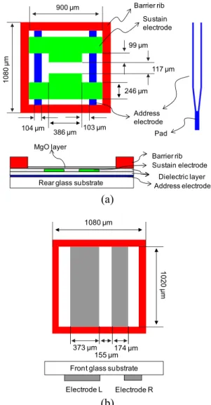
To verify the device concept, we have fabricated a MPCS panel of 100 mm × 100 mm without OLEDs, in which its cell pitch is 1080 µm × 1080 µm. The schematic drawings and dimensions of the unit cell are shown in Fig. 2.
Using photosensitive silver paste, a pair of parallel address electrodes with one pad electrode was formed at a width of 104 µm in each of the cells on a rear glass substrate, and covered by a dielectric layer with a thickness of 23 µm. Using the same silver paste and dielectric material, a pair of segmented sustain electrodes was patterned in each of the cells on the dielectric layer, and covered with another dielectric layer. They had a discharge gap of 117 µm, width of 246 µm, segmented length of 386 µm, and segmented width of 99 µm. The segmented sustain and address
electrodes were arranged perpendicular to each other, and had a discharge gap of 103 µm. Closed barrier ribs were formed at a thickness of 140 µm on the latter dielectric layer, and had a top width of 60 µm and bottom width of 180 µm. Finally, MgO was deposited at a thickness of 0.6 µm by electron beam evaporation. Using photosensitive silver paste, on a front glass substrate formed was a pair of parallel electrodes of different size denoted by electrodes L and R. The electrodes L and R were 373 µm and 174 µm in width, respectively. The electrodes L and R were separated from each other by a distance of 155 µm. Making the electrodes L and R cross the sustain electrodes at right angles, the front and rear glass substrates were assembled, exhausted, and filled with a mixture of He-Ne-Xe (50%-40%-10%) gases at a pressure of 100 Torr.
Barrier rib Dielectric layer Address electrode Rear glass substrate
Sustain electrode MgO layer 99 µm 386 µm 246 µm Barrier rib Sustain electrode Address electrode 900 µm 104 µm 117 µm 103 µm 10 80 µ m Pad (a)
Front glass substrate Electrode R Electrode L 102 0 µ m 1080 µm 373 µm 174 µm 155 µm (b)
Fig. 2. Schematic drawings and dimensions of the unit cell. Top and cross-sectional views of the unit
P1-99 / J. Y. Cai
• IMID 2009 DIGEST
4. Results and discussion
We first investigated discharge characteristics in a static operation. Changing peak voltage, AC voltage pulses with a square waveform were applied between the sustain electrodes at a frequency of 50 kHz and duty ratio of 30% while a DC biasing voltage of 18 V was applied between the electrodes L and R using two 9 V batteries. The cells started to be ignited from 245 V to 260 V, and the minimum sustain voltage was measured to be 215 V; thus, the static voltage margin was 30 V. This indicates that one of the device concepts, matrix addressing is attainable. Moreover, the discharge characteristics are barely changed even though the batteries are removed or the DC biasing voltage is increased to 27 V. They seem to be hardly affected by the DC biasing voltage because its magnitude is relatively small. When the AC voltage pulses were applied between the address and sustain electrodes, the cells started to be discharged from 250 V to 268 V.
To verify the other device concept, current switching, we used an inorganic light-emitting diode (LED) and two 9 V batteries connected in series to the electrodes L and R, as shown in Fig. 3. As illustrated in Figs. 3(a) and (b), while the LED is off when plasmas are turned off, the LED is on when they are turned on. This implies that the current switching is achievable.
(a) (b)
Fig. 3. Current switching. (a) An inorganic
light-emitting diode (LED) and two 9 V batteries are connected in series to the electrodes L and R. (b) The LED is turned on as the plasmas are initiated in a bunch of the cells which are addressed and sustained.
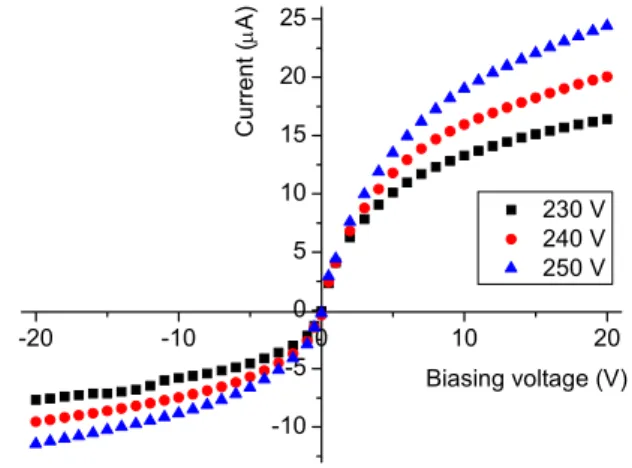
Finally, we measured the current-voltage (I-V) characteristic of the unit cell. Since stray capacitance to ground in a measurement circuit may produce displacement currents due to AC voltage pulses for plasma generation, AC bipolar voltage signals with positive and negative pulses of equal amplitude were applied to one of the paired sustain electrodes, and
synchronously applied to the other in opposite phase. The I-V measurements were carried out with a Keithley 2400 source-measure unit connected directly to the electrodes L and R. Applying AC bipolar voltage signals with a frequency of 100 kHz and duty ratio of 30%, we measured the current against the biasing voltage of the electrode R with respect to the electrode L for three different peak-to-peak voltage levels of 230 V, 240 V, and 250 V, as shown in Fig. 4.
In principle, the scheme of the electrodes L and S is equivalent to that of an asymmetric floating double probe with unequal areas except for their relative dimensions to the plasma volume [7, 8]. Accordingly, the I-V characteristic can be qualitatively analyzed by a floating double probe theory. Like a floating double probe, the current increases and saturates as the biasing voltage increases. And, the saturation current is larger when the bigger one of electrodes L and R is negatively biased than when it is positively biased, which indicates that the current is limited by ion saturation current. Furthermore, the saturation current increases as increasing peak-to-peak voltage, which seems to be attributed to the increase of plasma density and electron temperature.
Fig. 4. I-V characteristic of the unit cell. The
current is measured against the biasing voltage of the electrode R with respect to the electrode L for three different peak-to-peak voltage levels of 230 V, 240 V, and 250 V.
5. Summary
The concept of a microplasma current switch for a device operated in a current mode like organic light-emitting diodes, which features matrix addressability and current switching, is presented as well as its architecture and operational principle. To verify the concept, we have fabricated a 100 mm x 100 mm
-20 -10 0 10 20 -10 -5 0 5 10 15 20 25 230 V 240 V 250 V C urre nt ( µ A) Biasing voltage (V)
P1-99 / J. Y. Cai
IMID 2009 DIGEST • microplasma current switch panel in which its cell
pitch is 1080 µm x 1080 µm. The matrix addressability, current switching, and consequently feasibility are confirmed. The current-voltage characteristic of the unit cell is identical to that of an asymmetric double probe. The saturation current increases with driving voltage.
6. References
1. A. Sobel, IEEE Trans. on Plasma Sci., 19, p.1032 (1991).
2. H. Uchiike, and T. Hirakawa, IEEE-IAS Annual
Meeting, Vol. 1, p.45 (2003).
3. T.-F. Wu, C.-C. Chen, C.-C. Chen, and W.-F. Hsu,
IEEE Trans. Plasma Sci., 31, p.272 (2003).
4. T. Kakizaki, S. Tanamachi, and M. Hayashi, J. Soc.
Inf. Display, 5/1, p.57 (1997).
5. A. Nathan, G. R. Chaji, and S. J. Ashtiani, J.
Display Technol., 1, p.267 (2005).
6. D. Pribat, and F. Plais, Thin Solid Films, 383, p.25 (2001).
7. E. O. Johnson, and L. Malter, Phy. Rev., 80, p.58 (1950).