34-2 / H. Lee
IMID 2009 DIGEST •
Abstract
Color stable and efficient two wavelength white organic light emitting diodes (OLEDs) were fabricated using a iridium(III)[bis(4,6-difluorophenyl)-pyridinato-N,C2’]
picolinate (FIrpic) as a blue phosphorescent emitter and a bis(1-phenylisoquinolinato-C2,N)iridium (acetylacetonate)
((piq)2Ir(acac)) as a red phosphorescent emitter. The
emitting layers consist of two blue emitting layers and one red emitting layer which is between the two blue layers. The device reaches the peak efficiencies of 7.84 % and 10.3 cd/A at 0.6 mA/cm2. Furthermore, there
was little change of EL spectra according to current density change in the device .
1. Introduction
Recently, there has been increasing interest in white OLEDs for their potential use in full color display and solid state lighting sources.[1-3] Many researchers have
studied white OLEDs to improve the efficiency[4] and
the color stability[5]. Various structures of white
OLEDs have been used to improve the performance of the device such as doping several dopant into one or more emitting layer,[5] insertion the interlayer into the
emitting layer[6,7]. However, these methods are
complex to fabricate the device and difficult to achieve maximum efficiency of the device. In the case of multiple emissive layer, the efficiency of the device is high, but the color stability is not good.[8] One of the
methods to improve the efficiency and the color stability at the same time is to form a charge confinement in the desired emissive region.[9,10]
In this paper, we demonstrate the white OLEDs with charge confinement structure. The structure of this device is very simple because we use a single-host and a two wavelength system which has one red emission layer between two blue emission layers. But the device is very color stable and efficient.
2. Experimental
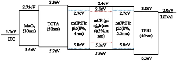
The white OLEDs device structure and energy levels of the materials used in this study are shown in Fig. 1. The device structure is as follows: indium-tin-oxide (ITO) as an anode/MoO3 (10 nm) as a hole injection
layer (HIL)/4,4’,4”-tri(N-carbazolyl) triphenylamine (TCTA, 50 nm) as a hole transport layer (HTL)/ 1,3-bis(9-carbazolyl)benzene (mCP):FIrpic (8 %, 4 nm) as a blue emitting layer/mCP:(piq)2Ir(acac) (3 %, x nm) as
a red emitting layer/mCP:FIrpic (8 %, 5.5 nm) as a blue emitting layer/2,2’,2”(1,3,5-benzenetriyl) tris-(1-phenyl-1H-benzimidazole (TPBi, 40 nm) as an electron transport layer/LiF(0.5 nm)/Al (100 nm) as a cathode. To optimize the efficiency and color stability, we change the thickness of the red emitting layer. The energy levels of MoO3 and TCTA are obtained from
the ultraviolet photoelectron spectroscopy and the UV-Visible spectroscopy. The energy levels of other materials are obtained from the literatures.[8,11-13]
Fig. 1. The white OLED structures used in this experiment and energy level diagram.
All the layers in these devices were prepared by thermal evaporation onto the ITO substrates. The substrates were ultrasonically cleaned by dipping them into various solvents. Organic and metal evaporation were conducted under a base pressure of 5×10⁻⁶ Torr without breaking the vacuum, and the
Color stable and efficient white organic light emitting
diodes with phosphorescent emitters
Hyunkoo Lee1 and Changhee Lee*1
1School of Electrical Engineering and Computer Science, Inter-University Semiconductor
Research center, Seoul National University, Seoul 151-744, Korea
Tel.:+82-2-880-9093, E-mail: [email protected]
34-2 / H. Lee
• IMID 2009 DIGEST
evaporation rates were 0.5-1.5 Å/s for the organic materials and 2-4 Å/s for the metal. The doping concentration was adjusted by varying the relative evaporation rates of the host and dopant materials, and the evaporation rates were monitored with a quartz-oscillator thickness monitor. The current-voltage (I-V) characteristics were measured by a Keithley-236 source measurement unit, and the luminance and electroluminescence spectra were obtained using a calibrated Si photodiode (Hamamatsu S5227-1010BQ) and CS 1000 spectrophotometer.
3. Results and discussion
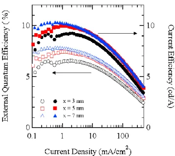
For more color stability and high efficiency, we change the thickness of red emitting layer as 3, 5, 7 nm. Figure 2 shows the external quantum efficiency and the current efficiency of these devices. The external quantum efficiency is 7.84 % and the current efficiency is 10.4 cd/A at 0.6 mA/cm2 in the x=7 nm
device. The device with thick red emitting layer has more high efficiency because the recombination region is expanded and this increases the probability of exciton formation.
Fig. 2. External quantum efficiency and current efficiency graphs of the devices (x is a red emitting layer thickness).
Fig. 3 (a) EL spectra and (b) CIE color coordinates of x = 7 nm device according to current density.
In our device structure, holes and electrons are trapped in the red emitting layer. Because the doping ratio of the red emitting layer is low relative to blue doping ratio, the change of red emission is small according to current density change. The barrier from (piq)2Ir(acac) to FIrpic is 0.5 eV for holes and 0.1 eV
for electrons. For holes, this barrier is very high. This limit the hole injection from red emitting layer to blue emitting layer and make little change of blue peaks
34-2 / H. Lee
IMID 2009 DIGEST •
according to the current density change. Consequently, the increase of red and blue emission is limited and the amount of color change is very small according to current density change. In other words, our device structure improves the color stability according to current density change. Figure 3 shows the EL spectra and Commission Internationale de l’Éclairage (CIE) color coordinates of the x=7 nm device. All EL spectra were normalized to compare the relative change of blue and red emission peaks. There was little change of EL spectra and CIE color coordinates in the device according to the current density increase.
4. Summary
We fabricated the simple white OLEDs which consist of one red emitting layer that is between two blue layers. As red emitting layer thickness increases, the efficiency of the device increases. Furthermore, there was little change of EL spectra and CIE color coordinates according to the current density change in the device.
Acknowledgement
This work was supported by Seoul R&BD program (CR070048) and New Growth Engine Display Center, Ministry of Knowledge Economy (MKE), Korea.
5. References
1. A. Misra, P. Kumar, M N Kamalasanan, and Subhas Chandra, Semicond. Sci. Technol., 21, R35-R47
(2006).
2. D. Gupta, M. Katiyar, and Deepak, Optical Materials, 28, pp295-301 (2006).
3. B. W. D’Andrade, and S. R. Forrest, Adv. Mater., 16,
pp1585-1595 (2004).
4. S. Reineke, F. Lindner, G. Schwrtz, N. Seidler, K. Walzer, B. Lüssem and K. Leo, Nature, 459,
pp234-238 (2009).
5. Q Wang, J. Ding, D. Ma, Y. Cheng, L. Wang and F. Wang, Adv. Mater. , 21, pp2397-2401 (2009).
6. Yiru Sun, Noel C. Giebink, Hiroshi Kanno, Biwu Ma, Mark E. Thompson and Stephen R. Forrest,
Nature, 440, pp908-912 (2006).
7. Unnat S. Bhansali, Huiping Jia, M. A. Quevedo Lopez, Bruce E. Gnade, Wei-Hsuan Chen, and Mohammad A. Omary, Appl. Phys. Lett., 94, 203501 (2009).
8. Yiru Sun and Stephen R. Forrest, Appl. Phys. Lett.,
91, 263503 (2007).
9. Shi-Jian Su, Eisuke Gonmori, Hisahiro Sasabe, and Junji Kido, Adv. Mater., 20, pp4189-4194 (2008).
10. J. H. Jou, Y. S. Chiu, R. Y. Wang, H. C. Hu, C. P. Wang, and H. W. Lin, Org. Electron., 7, pp8-15 (2005).
11. Heume-Il Baek and Changhee Lee, J. Appl. Phys.,
103, 124504 (2008).
12. Yen-Chun Chen, Guo-Sheng Huang, Chung-Chin Hsiao, and Show-An Chen, J. Am. Chem. Soc., 128, pp8549-8558 (2006).
13. Brian W. D’Andrade, Russel J. Holmes, and Stephen R. Forrest, Adv. Mater., 16, pp624-628