Highly selective spectral response with enhanced responsivity of n -ZnO / p -Si radial
heterojunction nanowire photodiodes
Han-Don Um, Syed Abdul Moiz, Kwang-Tae Park, Jin-Young Jung, Sang-Won Jee, Cheol Hyoun Ahn, Dong Chan Kim, Hyung Koun Cho, Dong-Wook Kim, and Jung-Ho Lee
Citation: Applied Physics Letters 98, 033102 (2011); doi: 10.1063/1.3543845 View online: http://dx.doi.org/10.1063/1.3543845
View Table of Contents: http://scitation.aip.org/content/aip/journal/apl/98/3?ver=pdfcov
Published by the AIP Publishing
Articles you may be interested in
p-Si nanowires/ SiO 2 /n-ZnO heterojunction photodiodes
Appl. Phys. Lett. 97, 013503 (2010); 10.1063/1.3462319
Response to “Comment on ‘Deep ultraviolet and near infrared photodiode based on n -ZnO / p -silicon nanowire heterojunction at low temperature’ ” [Appl. Phys. Lett.94, 166102 (2009)]
Appl. Phys. Lett. 94, 166103 (2009); 10.1063/1.3119200
Comment on “Deep ultraviolet and near infrared photodiode based on n -ZnO / p -silicon nanowire heterojunction at low temperature” [Appl. Phys. Lett.94, 013503 (2009)]
Appl. Phys. Lett. 94, 166102 (2009); 10.1063/1.3119197
Deep ultraviolet and near infrared photodiode based on n -ZnO / p -silicon nanowire heterojunction fabricated at low temperature
Appl. Phys. Lett. 94, 013503 (2009); 10.1063/1.3064161
Visible and ultraviolet light alternative photodetector based on ZnO nanowire/ n - Si heterojunction
Appl. Phys. Lett. 93, 163501 (2008); 10.1063/1.3003877
Reuse of AIP Publishing content is subject to the terms at: https://publishing.aip.org/authors/rights-and-permissions. Download to IP: 203.255.172.21 On: Wed, 06 Jul 2016 04:30:11
Highly selective spectral response with enhanced responsivity of
n-ZnO/ p-Si radial heterojunction nanowire photodiodes
Han-Don Um,1Syed Abdul Moiz,2Kwang-Tae Park,1Jin-Young Jung,2Sang-Won Jee,2 Cheol Hyoun Ahn,3Dong Chan Kim,3Hyung Koun Cho,3Dong-Wook Kim,4,a兲 and Jung-Ho Lee1,2,a兲
1Department of Bio-Nano Technology, Hanyang University, Ansan 426-791, South Korea
2Department of Materials and Chemical Engineering, Hanyang University, Ansan 426-791, South Korea 3
School of Advanced Materials Science and Engineering, Sungkyunkwan University, Suwon 440-746, South Korea
4
Department of Physics and Department of Chemistry and Nano Science, Ewha Womans University, Seoul 120-750, South Korea
共Received 18 November 2010; accepted 29 December 2010; published online 18 January 2011兲 A radial heterojunction nanowire diode共RND兲 array consisting of a ZnO 共shell兲/Si 共core兲 structure was fabricated using conformal coating of a n-type ZnO layer that surrounded a p-type Si nanowire. In both ultraviolet共UV兲 and visible ranges, the photoresponsivity of the RND was larger than that of a planar thin film diode 共PD兲 owing to the efficient carrier collection with improved light absorption. Compared to a PD, in the forward bias, a 6 m long RND resulted in a⬃2.7 times enhancement of the UV responsivity at =365 nm, which could be explained based on the oxygen-related hole-trap mechanism. Under a reverse bias, UV-blind visible detection was observed while the UV response was suppressed. © 2011 American Institute of Physics.
关doi:10.1063/1.3543845兴
One-dimensional semiconductor nanowires共NWs兲 have attracted much attention for use in optoelectronic applica-tions due to their unique optical and electrical properties.1–3 In particular, ZnO NWs are considered a promising material for light-emitting diodes, laser diodes, and photodetectors because ZnO NWs have a wide band gap 共3.37 eV兲, large exciton binding energy 共60 meV兲, and a high photoconduc-tivity gain.3 Since several key issues4such as deep acceptor levels and low dopant solubilities have prevented reproduc-ible fabrication of p-type ZnO for p-n homojunctions,
n-ZnO/p-Si heterojunctions have been intensively
investi-gated as an alternative approach.5–7
Heterojunction photodiodes demonstrate UV and visible photoresponses due to the large band offset at the interface with the significant difference in the band gaps of ZnO and Si. Mridha and Basak6 demonstrated that n-ZnO/p-Si thin film photodiodes could selectively detect either UV or visible photons by varying the applied bias. Although ZnO or Si NW structures have been introduced in previous studies7,8to obtain a high conductivity gain with a ZnO NW or strong light absorption with a Si NW, the entire NW surface has not been used as a junction region due to insufficient conformal deposition.
In this study, we demonstrate radial heterojunction NW photodiodes 共RNDs兲 consisting of p-Si/n-ZnO NW core/ shell structures which were fabricated using atomic layer deposition共ALD兲. Their photoresponse properties are antici-pated to provide insight for the formation of promising pho-todetector nanodevices. Conformal coating with a thin ZnO layer formed a depletion region on a several microns long Si NW across the entire interface area. The RND exhibited en-hanced UV and visible responsivities compared to a planar
thin film photodiode共PD兲. The photoresponse selectivity of a RND in the visible to UV range was found to be significantly enhanced compared to a PD. All of the experimental data can be understood based on the unique advantages of the RND geometry.
Figure1共a兲illustrates the configuration used for the pho-toresponse measurements of a RND. Vertically dense Si NW arrays were fabricated by Ag-induced electroless etching of
p-type Si wafers 共resistivity of 1–10 ⍀ cm兲.9 The NW length could be easily controlled by varying the etching time. After formation of the Si NW arrays, the ALD technique was used to conformably coat a n-type ZnO thin film on the high aspect ratio Si NWs.10A 100 nm thick ZnO layer was
depos-a兲Authors to whom correspondence should be addressed. Electronic ad-dresses: [email protected] and [email protected].
FIG. 1. 共Color online兲 共a兲 Schematic showing the configuration of the pho-toresponse measurement system used for the n-ZnO共shell兲/p-Si共core兲 radial nanowire photodiodes. 共b兲 A typical cross-sectional SEM image of the
n-ZnO/p-Si NW arrays. 共c兲 A magnified image showing the bottom region
of a ZnO/Si NW, in which the ZnO shells were partly peeled off during the sample preparation. A uniform thickness of ZnO over the Si core is ob-served. The yellow dashed lines indicate the position of the interface be-tween ZnO and Si. 共d兲 A scanning TEM image with 关共e兲 and 共f兲兴 two-dimensional energy dispersive x-ray spectroscopy mapping of Zn共green兲, O 共white兲, and Si 共purple兲.
APPLIED PHYSICS LETTERS 98, 033102共2011兲
0003-6951/2011/98共3兲/033102/3/$30.00 98, 033102-1 © 2011 American Institute of Physics
Reuse of AIP Publishing content is subject to the terms at: https://publishing.aip.org/authors/rights-and-permissions. Download to IP: 203.255.172.21 On: Wed, 06 Jul 2016 04:30:11
ited at 150 ° C to form the n-ZnO/p-Si NW junctions. The standard resistivity and carrier concentration were measured to be 4.6⫻10−3 ⍀ cm and 5.1⫻1019 cm−3, respectively, on
ZnO thin films deposited under identical conditions on glass substrates. Top and bottom electrodes were formed using 250 nm thick Al thin films which were evaporated both on the front 共ZnO兲 and substrate backside. The properties of long 共6 m兲 and short 共2 m兲 nanowire photodiodes, denoted as RND2 and RND6, respectively, were compared to a PD. The aspect ratios of the RNDs, which were calculated using the averaged values of the lengths and diameters, were⬃10 and 30 for RND2 and RND6, respectively.
The typical diameter of the n-ZnO/p-Si NW arrays was 350–400 nm, which consisted of a 100 nm thick shell and a 150–200 nm thick NW core关Figs.1共b兲 and1共c兲兴. All of the ZnO/Si heterojunction devices exhibited nonlinear rectifying behaviors in their I − V characteristics共inset in Fig.2兲 but the overall measured current levels under forward and reverse biases were higher in the RNDs than in the PD due to the increased junction area. The presence of interface states is also known to increase the reverse current, i.e., leakage current.6,7Further analysis of the logarithmic plots共Fig.2兲 of the I − V data suggests a clear difference between the trans-port behaviors of the RNDs and PD. The forward bias cur-rent exponentially increased in the PD according to the rela-tionship of I⬀exp共␣V兲 due to the recombination-tunneling
mechanism7in the wide band gap p-n heterojunction. On the other hand, two different regions depending on the bias level were observed in the RNDs.
For the very low bias range 共region I兲 of 0⬍V ⬍0.8 V, almost the same rectifying behavior as a PD was observed with the RNDs due to the recombination-tunneling mechanism. However, the I − V behavior normally followed the relationship of I⬀共V−V0兲2 for the high bias range of V
⬎0.8 V 共region II兲. This may be attributed to the space-charge-limited current 共SCLC兲 conduction, which has often been observed in semiconductor nanostructures including thin films.7 The SCLC effect was reported11 to be greatly amplified in cases using NWs, in which inherent geometrical and material issues such as poor electrostatic screening in high-aspect ratio structures, enhanced carrier depletion due to surface states, and charge traps incorporated during the nanostructure growth are influential. The higher levels of the reverse current and SCLC conduction observed in the RNDs
corroborate the notion that the increased ZnO/Si interfacial area mostly operated as radial heterojunctions.
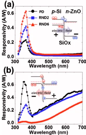
The energy band diagrams of the ZnO/Si heterojunction under forward and reverse biases are depicted in the insets of Figs. 3共a兲 and3共b兲, respectively. Given the band gaps and electron affinities of ZnO and Si,5a valence band offset共2.55 eV兲 greater than the conduction band offset 共0.4 eV兲 is ex-pected for a n-ZnO/p-Si heterojunction. Figure 3共a兲shows the photoresponsivity spectra under a forward bias of 0.5 V. Since the transmittance of ZnO on a glass substrate was mea-sured to be over 80% in the visible range 共400–700 nm兲, visible light is normally absorbed in the underlying p-Si after passing through the ZnO layer. The absorbed light generates electron-hole pairs 共EHP兲 inside the Si. The electric field drives the photogenerated holes toward the n-ZnO side, but they cannot cross over the SiO2 layer between p-Si and
n-ZnO due to the high potential barrier for holes, as shown in
the inset of Fig. 3共a兲. Thus, the visible photoresponsivity is mainly attributed to the transport of photogenerated electrons 共minority carriers兲 in p-Si, which is very low in magnitude. The photoresponsivity remained nearly constant in the vis-ible range共400–700 nm兲 for all samples.
In contrast with the response to visible light, the photo-responsivity spectra with UV exposure showed a strong re-sponse under a forward bias. Since the penetration depth of UV light is less than 100 nm in ZnO, most photons from the UV light are absorbed in the ZnO layer. The strong UV re-sponse can be explained by the different drift behaviors of the electrons 共photogenerated in ZnO兲 and holes 共photoge-nerated in Si兲. The electrons photogenerated in ZnO can eas-ily move to Si due to the relatively low potential barrier at
FIG. 2.共Color online兲 Logarithmic I−V plots of the RNDs and PD. For the RNDs, “I” and “II” refer to the regions dominated by the different transport behaviors with the applied bias. Linear I − V plots are also shown in the inset.
FIG. 3.共Color online兲 Photoresponsivity spectra of the RNDs and PD mea-sured under共a兲 forward and 共b兲 reverse biases. Their energy band diagrams and charge transport mechanisms are also depicted in the insets.
033102-2 Um et al. Appl. Phys. Lett. 98, 033102共2011兲
Reuse of AIP Publishing content is subject to the terms at: https://publishing.aip.org/authors/rights-and-permissions. Download to IP: 203.255.172.21 On: Wed, 06 Jul 2016 04:30:11
the interfacial region while the photoholes in Si cannot tun-nel through the high potential barrier.5,6
In addition, the UV responsivities of RND2 and RND6 are higher than that of the PD under a forward bias. Soci et
al.3reported that the enhanced UV photoconductive response in ZnO NWs could be attributed to the presence of oxygen-related hole-trap states at the NW surface. The trap states can prolong the photocarrier lifetime while preventing charge-carrier recombination 共hole-trapping mechanism兲. Photo-holes are readily trapped by the negatively charged oxygen ions, leaving behind unpaired electrons which are either col-lected at the electrode or recombine with holes. As a result, RNDs can improve the UV photodetection sensitivity due to the high surface area to volume ratio. Figure 3共a兲confirms that the forward bias UV responsivity was improved by in-creasing the NW length 共increased surface area to volume ratio兲, in which the UV responsivities at =365 nm were detected to be 0.23, 0.42, and 0.63 A/W for PD, RND2, and RND6, respectively. In the wavelength range of 300–365 nm, the UV responsivities drastically decreased with de-creasing wavelength since the penetration of high energy photons became very short 共⬍40 nm兲.5 Due to the short penetration depth, the carrier generation normally occurs near the surface. Significant surface scattering and recombi-nation decrease the carrier lifetime.
Note that the UV photoresponse of RNDs under a re-verse bias shown in Fig. 3共b兲 is significantly suppressed compared to the PD. The visible/UV responsivity ratios cal-culated using the responsivities measured at=700 and 365 nm were 17.2 for RND6 and 0.86 for PD. A previous work3 reported that the ZnO surface can be depleted by the surface oxygen absorption according to the hole-trapping mecha-nism. For the forward bias, carrier depletion behavior at the NW surface is beneficial for photoelectrons to transport from ZnO to Si via the effective carrier separation. Under a re-verse bias, however, the surface depletion of ZnO acts as a diffusion barrier for photoelectrons to collect at the top elec-trodes. This feature causes the electrons to suffer from seri-ous recombination, which finally results in a remarkable sup-pression of the UV photoresponse with increasing NW length.
In contrast with the forward bias, a monotonous increase with increasing wavelength was observed in the visible re-sponse results共400–700 nm兲 under a reverse bias. The inci-dent visible light can generate EHPs in the p-Si layer where the photogenerated electrons and holes under the reverse bias move to the ZnO and Si sides, respectively. The radial het-erojunction geometry is known to help efficient carrier col-lection and light trapping.1,2Contrary to the expectation, the visible photoresponsivities of the RNDs were observed to be similar to or even lower than that of the PD. This can be explained by the morphology of the highly dense ZnO/Si NW arrays. The ZnO thickness normally increases closer to
the NW bottom region due to overlaying of the ZnO shells via merging of adjacent wires during ZnO deposition, as shown in Figs.1共a兲and1共b兲. Increasing the ZnO thickness at the NW bottom degrades the visible transmittance,12 which results in the inferior light absorption in Si. Given that a similar visible responsivity to the PD was observed in RND2, the actual responsivity of the RND, which has a thicker ZnO layer at the NW bottom under the same coating condition, is also estimated to be higher than that of the planar counterpart.
In conclusion, we fabricated n-ZnO/p-Si RNDs using metal-assisted electroless etching of Si and conformal coat-ing of ZnO by an ALD process. Compared to a planar ZnO/Si heterojunction, both the UV and visible photorespon-sivities of the RNDs were enhanced, owing to the enlarged surface area to volume ratio, efficient carrier collection, and improved light absorption. In addition, our RNDs exhibited either UV-blind visible or visible-blind UV photoresponse, depending on the bias polarity. All of the advantageous char-acteristics of the RNDs can be further improved by optimiz-ing the device design and fabrication processes.
This work was supported by the Pioneer Research Cen-ter Program共Grant No. 2010-0002231兲 and Nano R&D Pro-gram 共Grant No. 20090083229兲 through the National Re-search Foundation grant funded by the Ministry of Education, Science and Technology. This work was sup-ported by the New and Renewable Energy of the Korea In-stitute of Energy Technology Evaluation and Planning grant funded by the Ministry of Knowledge Economy共Grant No. 2009T100100614兲. H.-D.U., K.-T.P., and S.-W.J. acknowl-edge financial support of the fifth-stage Brain Korea 21 Project in 2010.
1B. M. Kayes, H. A. Atwater, and N. S. Lewis,J. Appl. Phys. 97, 114302 共2005兲.
2E. Garnett and P. Yang,Nano Lett. 10, 1082共2010兲.
3C. Soci, A. Zhang, B. Xiang, S. A. Dayeh, D. P. R. Aplin, J. Park, X. Y. Bao, Y. H. Lo, and D. Wang,Nano Lett. 7, 1003共2007兲.
4Y. Ma, G. T. Du, S. R. Yang, Z. T. Li, B. J. Zhao, X. T. Yang, T. P. Yang, Y. T. Zhang, and D. L. Liu,J. Appl. Phys. 95, 6268共2004兲.
5I.-S. Jeong, J. H. Kim, and S. Im,Appl. Phys. Lett. 83, 2946共2003兲. 6S. Mridha and D. Basak,J. Appl. Phys. 101, 083102共2007兲.
7S. Y. Liu, T. Chen, Y. L. Jiang, G. P. Ru, and X. P. Qu,J. Appl. Phys. 105, 114504共2009兲.
8C. Y. Huang, Y. J. Yang, J. Y. Chen, C. H. Wang, Y. F. Chen, L. S. Hong, C. S. Liu, and C. Y. Wu,Appl. Phys. Lett. 97, 013503共2010兲. 9H. D. Um, J. Y. Jung, H. S. Seo, K. T. Park, S. W. Jee, S. A. Moiz, and
J.-H. Lee,Jpn. J. Appl. Phys., Part 1 49, 04DN02共2010兲.
10B. H. Kong, M. K. Choi, H. K. Cho, J. H. Kim, S. Baek, and J.-H. Lee,
Electrochem. Solid-State Lett. 13, K12共2010兲.
11A. A. Talin, F. Léonard, B. S. Swartzentruber, X. Wang, and S. D. Hersee,
Phys. Rev. Lett. 101, 076802共2008兲.
12X. Yu, J. Ma, F. Ji, Y. Wang, C. Cheng, and H. Ma,Appl. Surf. Sci. 245, 310共2005兲.
033102-3 Um et al. Appl. Phys. Lett. 98, 033102共2011兲
Reuse of AIP Publishing content is subject to the terms at: https://publishing.aip.org/authors/rights-and-permissions. Download to IP: 203.255.172.21 On: Wed, 06 Jul 2016 04:30:11