1018
-Abstract - Recently, standby power reduction techniques ofAC/DC adaptor were developed, consuming power almost arrived to 300㎽ level. The standby power losses are composed of the input filter loss 11.8㎽, the control IC for AC/DC adaptor 18㎽, the switching loss 9.53㎽ and the feedback loss 123㎽. And there are the standby power reduction techniques. In this paper, in order to reduce the standby power of SMPS more, the loss due to a voltage difference between input and output is reduced by the control circuit which is composed of the low voltage driving circuit and voltage regulator. The low voltage driving circuit operates on the low voltage of input and off the high voltage. The low voltage driving IC was produced by the 1.0㎛, high voltage DMOS process.
1. Introduction
International Energy Agency announced that the standby power of OECD member country is 10% level of power consumption per house. In the case of USA, the 5% of total electrical power consumption is the standby power and when changes money reaches to 1.3 billion dollar. Total standby power of Korea house is about 618MW and power that will be able to supply to 1.2 million house, and correspond to one thermal power generation.
And each country consider many kind method to reduce the standby power, energy star program in USA and EuP Tier program in EU recommend the standby power level as 50㎽ of AC/DC adaptor. The standby power of fly-back converter with under 5W is reached to 3㎽ by PI. The standby power of under 5㎽ is regarded as 0W in IEC 62301
Recently, standby power reduction techniques of AC/DC adaptor were developed, consuming power almost arrived to 300㎽ level. The standby power losses are composed of the input filter loss 11.8㎽, the control IC for AC/DC adaptor 18㎽, the switching loss 9.53㎽ and the feedback loss 123㎽[1].
Fig 1 shows the relationship of input power and output power, the smaller output and input power, the lower efficiency. It is necessary to upgrade the efficiency of fly-back converter on the light load. This is how to reduce the standby power of the fly-back converter of which consumer electronics are composed.
<Fig 1> No-load and standby power efficiency There is a various standby power reduction method that is (1) Reduction of power consumption in startup resistor [4,5],
(2) Reduction of switching frequency[3,7], (3) Reduction of output voltage disconnection, (4) Output voltage drop, (5) Use of a low-power auxiliary power supply [3]. Other proposals also include using burst mode [3,6,7] to keep the dc link voltage steady, the design of low-loss semiconductor integrated circuits [8-10] and adoption of control mechanism [7] and algorithm for standby power reduction.
Fig 2 show typical SMPS circuit and the power consumption of EMI filter is 11.8㎽, control IC 18㎽, switching loss 9.53㎽ and feedback loss 123㎽ at each part on the standby mode. Total standby power of SMPS is 165㎽.
<Fig 2> Standby power loss in each part of SMPS In this paper, in order to reduce the standby power of SMPS more, the loss due to a voltage difference between input and output is reduced by the control circuit which is composed of the low voltage driving circuit and voltage regulator.
2. Proposed standby power reduction circuit 2.1 Proposed circuit for minimization of standby power
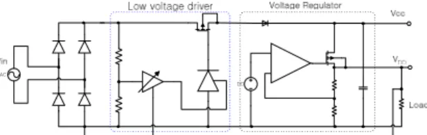
To reduce the standby power of SMPS more, the loss due to a voltage difference between input and output is reduced by the control circuit in Fig 3. Proposed circuit is composed of the low voltage driving circuit and voltage regulator. The low voltage driving circuit operates on the low voltage of input and off on the high voltage input. Circuit operation principle is as in the following.
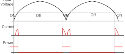
<Fig 3> Proposed circuit to reduce the standby power Comparator of low voltage driver feed voltage of resistor divider in Fig 3 and set value, if feeding voltage > set value, output 2.5V high voltage on the comparator and shunt regulator is commuted, power MOSFET is turned off. If feeding voltage < set value, output 0V voltage on the comparator and shunt regulator is turned off, power MOSFET is turned on. Thus proposed circuit supply power in the case of feeding voltage > set value as waveform of Fig 4. Fig 4 is
대기전력 최소화를 위한 교류전압 입력에 따른 저전압 구동회로 설계
서길수*, 김기현*, 김형우*, 이경호*, 김종현* 전력반도체연구센터 한국전기연구원
Standby Power Reduction Technique due to the Minimization of voltage difference
between input and output in AC 60㎐
Kil-Soo Seo*, Ki-Hyun Kim*, Hyung-Woo Kim*, Kyung-Ho Lee*, Jong-Hyun Kim* Power Semiconductor Research Center, Korea Electrotechnology Research Institute*
1019
-shown that the waveform of input voltage, current and power.So the loss due to voltage difference between input and output is reduced and the standby power is reduced.
ON Off ON Off ON
Input Voltage
Current
Power
<Fig 4> Input voltage, current and power waveform of proposed circuit
The low voltage driving IC was produced by the 1.0㎛, high voltage DMOS process. Fig 5 is shown that three core chips are in a die.
<Fig 5> Manufactured chip layout of proposed circuit 2.2 Simulation and experimental results
Fig 6 shows the result that are output voltage, output current and input current depended upon time on the left side of figures, input power, output current and output voltage depended upon resistance of load on the right side. The bottom on the left side of Fig 6 similar with the current waveform of Fig 4. It is confirmed that the proposed circuit is operated well.
<Fig 6> Electrical characteristics of proposed circuit by simulation
Fig 7 show the input voltage and current waveform on the left side output voltage and input voltage at load 5.6㏀.
<Fig 7> Waveform @ load 5.6㏀, Vout=7.7V
Fig 8 shows the waveform of input voltage, output voltage and current at load 5.6㏀ and MLCC 9.4㎌.
<Fig 8> Waveform @ load 5.6㏀, Vout=7.7V It was confirmed that the proposed circuit operate well by the testing of manufacturing chip.
3. Conclusion
In this paper, in order to reduce the standby power of SMPS more, the loss due to a voltage difference between input and output is reduced by the control circuit which is composed of the low voltage driving circuit and voltage regulator. The low voltage driving circuit operates on the low voltage of input and off the high voltage. The low voltage driving IC was produced by the 1.0㎛, high voltage DMOS process. Proposed standby power reduction circuit with low voltage difference between input and output was confirmed by testing chip.
Acknowledgement
This work was supported by the Energy efficiency & Resources Core Technology program of the Korea Institute of Energy Technology Evaluation and Planning(KETEP) granted financial resource from the Ministry of Trade, Industry & Energy, Republic of Korea(No .2013020101530)
[References]
[1] Byoung-Hee Lee, Ki-Bum Park, Chong-Eun Kim and Gun-woo Moon, “No-Load power reduction techniques for AC/DC Adaptors”, IEEE Transactions on Power Electronics, Vol. 27, No 8, August 2012.
[2] Hang-Seok Choi, Huh, D.Y. “Techniques to minimize Power Consumption of SMPS in Standby Mode” IEEE 36th Power Electronics Specialists Conference, 2005. PESC '05. 2005 Page(s) 2817∼2822
[3] Yau, Y.T. Hwu, K.I. Yung-Shan Chou, ”Reducing standby power applied to SR forward converters with transient load response considered”, The 2004 47th Midwest Symposium on Circuits and Systems, 2004. MWSCAS '04. Volume 2, 25∼28 July 2004 Page(s) 313∼316
[4] Yu-Kang Lo, Shang-Chin Yen, Chung-Yi Lin, “A High-Efficiency AC/DC Adaptor With a Low Standby Power Consumption”, IEEE Transactions on Industrial Electronics, Volume 55, Issue 2, Feb. 2008 Page(s), 963∼965.
[5] Joon Heo, Choong Seon Hong, Seok Bong Kang, Sang Soo Jeon, “Design and Implementation of Control Mechanism for Standby Power Reduction”, IEEE Transactions on Consumer Electronics, Volume 54, Issue 1, February 2008 Page(s), 179∼185
[6] LO Y.K., YEN S.C., LIN C.Y. “A high-efficiency AC/DC adaptor with a low standby power consumption”, IEEE Trans. Ind. Electron, 2008, IE-55, (2), pp. 963∼965
[7] Jung, J.H., Choi, J.M., Kwon, J.G, “Novel techniques of the reduction of standby power consumption for multiple output converters”. IEEE Annual Applied Power Electronics Conf. and Exposition(APEC’08), Austin, USA, 2008, pp. 1575∼1581
[8] Jin-ho Choi, Dong-young Hug, Young-seok Kim, "The improved burst mode in the stand-by operation of power supply", IEEE APEC'04. 19th Annual IEEE Volume 1, pp.426∼432 2004
[9] Bo-Teng Huang, Ko-Yen Lee, Yen-Shin Lai, "Design of a Two-Stage AC/DC Converter with Standby Power Losses Less than 1 W", Power Conversion Conference-Nagoya, 2007. PCC'07, 2007
[10] Y. K. Lo, S.C. Yen and C.Y. Lin, “A High-Efficiency AC/DC Adaptor With a Low Standby Power Consumption”, in IEEE Trans. Industrial Electronics. vol. 55, no. 2, pp. 963∼965, February, 2008.