55-3 / H. S. Shin
• IMID 2009 DIGEST
Abstract
We have fabricated inverted staggered pentacene Thin Film Transistor (TFT) with 1-µm channel length by micro contact printing (µ-CP) method. Patterning of micro-scale source/drain electrodes without etching was successfully achieved using silver nano particle ink, Polydimethylsiloxane (PDMS) stamp and FC-150 flip chip aligner-bonder. Sheet resistance of the printed Ag nano particle films were effectively reduced by two step annealing at 180 oC.
1. Introduction
The patterning of thin film with maskless and soluble process has become an important part of the recent Organic Thin Film Transistors (OTFTs) applications such as smart card, radio frequency identification (RFID) tags, active matrix liquid crystal displays (AM-LCD) and active matrix organic light emitting diode display (AM-OLED).1-4 OTFTS are suitable for the process of low cost, low-temperature, and the large area electronic applications. The thin film pattering methods with conventional vacuum deposition and photolithographic process are too
expensive and complex.8 Thus, OTFTs are
manufactured by many direct printing techniques including inkjet printing (IJP) 1-2, screen printing 3, micro contact printing (µ-CP) 4-7, nano imprint lithography (NIL) 9-10, and laser printing (LP).11
In recent, IJP method is frequently used by maskless direct patterning, but it is very difficult to provide micro pattern size below 10 µm in organic layer due to some drawbacks such as the limited ink formulation, the inkjet nozzle size and the limitation of viscosity
control for solution.1-3 The NIL technique always needs an additional etching process due to residual layer, though it can define sub-50 nm size patterns.9 The laser patterning method is an emerging technique for controlling the pattern width below 10 µm by changing the beam spot sizes.11 The µ-CP method is the most effective technique for the direct micro patterning below 5-µm without vacuum process. Recently, an OTFTs having a channel length of 2 µm has been reported. However, it is also difficult to fabricate large area pattern.4-7
In this study, the source/drain electrodes having 1-µm gap width (which defines the OTFT channel length) have been patterned by µ-CP method with Ag nano-particle ink and Polydimethylsiloxane (PDMS) stamp using FC-150 Flip Chip Aligner-bonder (Karl Suss). Sheet resistance and surface roughness of the printed Ag films were investigated as function of annealing temperature. The electrical properties of 1-µm channel length pentacene TFTs with direct printed source/drain electrodes were also investigated.
2. Experimental
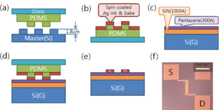
Figure 1 shows the flow schematic diagram of the fabrication process for OTFTs with Ag nano-particle ink as source and drain electrodes in the case of top-contact (TC) configuration OTFTs. We prepared the silicon master using conventional photolithography method and etching process with 1.8 µm depth. The PDMS (Dow Corning Sylgard-184) stamp was fabricated using this master [Fig.1(a)]. The PDMS solution was thoroughly mixed 10:1 (Sylgard 184 A:
Fabrication of 1-µm channel length OTFTs by
micro-contact printing
Hong-sik Shin
1,2, Kyu-ha Baek
1, Ho-jin Yun
1,2, Yong-hyun Ham
1, Kun-sik
Park
1, Ga-Won Lee
2, Hi-Deok Lee
2, Jin-suk Wang
2, Kijun Lee
2, and Lee-Mi Do
11
Electronic and Telecommunications Research Institute (ETRI), 305-700, Daejeon, Korea
2
Dept. of Electronics Engineering, Chungnam National University, 305-764, Daejeon, Korea
Tel.:82-42-860-5287, E-mail: [email protected], [email protected]
55-3 / H. S. Shin
IMID 2009 DIGEST • Fig. 1. Flow schematic diagram of our fabrication
process for TCOTFTs(a) A patterned PDMS mold
on a hard substrate using Si master. (b) Ag nano-particle ink is spin coated on the PDMS mold. (c) Pentacene layer deposited using thermal evaporation on SiN(100 nm)/Si substrate. (d) The PDMS mold coated with Ag nano particle ink is put in the SiN/Si substrate with Pentacene using FC-150 [(b)+(c)]. (e) PDMS mold was removed from the substrate, leaving the Ag source and drain pattern on Pentacene layer (Inverted staggered OTFT). (f) Optical microscope image of printed Ag source and drain using µ-CP on PES substrate (W/L=100 µm/1 µm).
Sylgard 184 B) and degassed in a desiccator for 30 minutes. Using vacuum pump, the poured PDMS on the Si master was degassed again to remove the trapped air bobbles, which were generated from the inside of the deep and narrow trench during the casting. For uniformity, the 1-mm-thick glass was adhered to PDMS solution in a µ-CP because PDMS mold had the flexibility. The PDMS mold was separated from the master and baked on a hotplate (110 oC, 10 min) for hardening. Ag nano-particle ink was spin coated on the PDMS mold (3000 rpm, 30 sec) and baked on a hotplate (120 oC, 30 sec) for weakly drying solvent [Fig. 1(b)]. Then, the 30 nm thick pentacene active layer was deposited on SiN (100 nm)/Si substrate by thermal evaporation under base pressure of 5×10⁻⁷ Torr. In order to obtain well-ordered pentacene film, the 2-steps deposition was used as follows; the thin 3 nm films was evaporated at a deposition rate of 0.3 nm/min and the other 27 nm thick pentacene was deposited with a relatively high deposition rate of 3.0 nm/min [Fig. 1(c)].
The PDMS mold coated with Ag nano particle ink is put on the SiN/Si substrate with Pentacene using FC-150. FC-150 can be applicable to more various applications because of its possibility of the alignment in the error range of ±0.1 µm and the formation of
uniform patterns in the uniform pressure [Fig. 1(d)]. Then, the PDMS mold coated with Ag nano particle ink is put on the SiN/Si substrate with Pentacene using FC-150. FC-150 can be applicable to more various applications because of its possibility of alignment in the error range of ±0.1 µm and formation of uniform patterns in the uniform pressure [Fig. 1(d)]. Then, the PDMS mold was removed from the substrate, leaving the Ag source and drain pattern on pentacene layer. Finally, the Ag layer was baked on hotplate (180 oC, 1 min) to dry solvent.
The current-voltage (I-V) characteristics of pentacene TFT was measured using HP 4156C Semiconductor Parameter Analyzer. Sheet resistance of Ag nano particle ink layer was measured using Four Point Probe System.
3. Results and discussion
Figure 2 shows the sheet resistance of Ag nano-particle ink film layer as functions of annealing temperature and duration time in atmosphere (Fig. 2(a)), and annealing temperature of 2-step annealing process (Fig. 2(b)) in atmosphere condition. It can be seen that the annealed sample below 120 oC exhibited the high sheet resistance (300 ohm/sq.), but the resistance abruptly decreased with increase of annealing temperature above 120 oC. In spite of the increase of duration time in atmosphere, the sheet resistance was maintained constant value. It is believed that Ag nano-particle ink film layer could be used as reliable source and drain electrodes of OTFT. In Fig. 2(b), the solid rectangular (■) represents that the samples were first annealed at the temperatures between room temperature and 300 oC. The samples marked as sold rectangular were reannealed at the
Fig. 2. Sheet resistance(Rsh) change of Ag nano
particle ink films (a) as a function of annealing
temperature and duration time in atmosphere, (b) as a function of annealing temperature of 2-step annealing temperature in atmosphere condition.
55-3 / H. S. Shin
• IMID 2009 DIGEST
Fig. 3. FE-SEM images of the samples fabricated using µ-CP process. (a) The length of source and drain electrode is about 0.5 µm, (b) the thickness is about 78nm (3000 rpm and 30 sec), (c) the changes of film thickness with spin speed.
temperatures of 160 (▽), 180 (○),and 200 (△) oC, respectively. The sheet resistances of the samples
annealed at below 120 oC were decreased after
secondly annealing at high temperatures. One the other hand, for the samples annealed at the high temperatures above 120 oC, the changes of resistances did not occur in spite of high-temperature second-annealing.
Optical microscope image of printed Ag layer using 1-step annealing in Fig. 2(a) shows that viscosity of Ag nano particle ink is very important during the µ-CP. The form of Ag electrode pattern was not clearly formed during the µ-CP using a low viscosity solution. Finally, we formed clearly Ag electrode pattern using 2-step annealing for controlled Ag nano particle ink viscosity [Fig. 1(f)].
Figure 3(a) shows the SEM image of the sample fabricated by µ-CP process. The length of source or drain patterns is about 0.5 µm. The thickness of the sample is about 78 nm in Fig. 3(b). Figure 3(c) shows the thickness change with spin speed. The thicknesses of second annealed samples were reduced to about half of those of the first annealed samples.
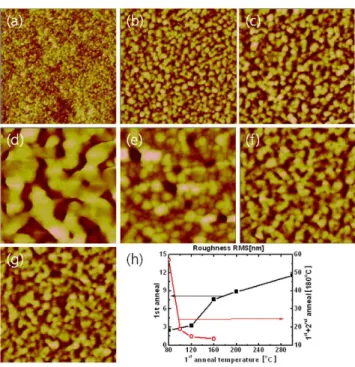
Figure 4 shows the AFM images of the Ag nano-particle ink electrode using µ-CP. It can be seen from Fig. 4(a) ~ (c) that RMS roughness increased with increasing temperature of the first annealing. As shown in Fig. 4(d) ~ (g), the first step annealing was
Fig. 4. AFM image (2 x 2 µm2) using µ-CP source
and drain electrodes with Ag nano-particle ink. First anneal (a) 80 oC (b) 160 oC (c) 200 oC, [ first anneal (d) 80 oC (e) 100 oC (f) 120 oC (g) 160 oC] +
second anneal (180 oC), (h) change of surface
roughness from 2-step anneal.
performed at 80, 100, 120, 160, and the second annealing was done at 180 oC. Roughness value is highest for the sample annealed at the lowest first annealing temperature of 80 oC.
Figure 5 shows the I-V characteristics of pentacene TFT with Ag source and drain electrodes with channel length of 1 µm and channel width of 1000 µm. We calculated field effect mobility (µ) using highest transconductance (Gm.max) point on linear region [Cox means the capacitance of SiN layer (3.36 nF/cm2 @ 1 kHz)]. The results are summarized in Table I. The field effect mobility (µFE) is 0.264 cm2/Vs, the threshold voltage (VT) is 0.032 V, the sub-threshold slop (SS) is 0.84 V/dec. and the on-off ratio is 2.93×10⁵.
4. Summary
Consequently, the general methods used a photolithography using mask and etching process or a patterning using shadow mask in vacuum progress are expensive and complex method, but this proposed µ -CP method is the most possible process for the low
55-3 / H. S. Shin
IMID 2009 DIGEST •
cost, the low-temperature and the effective pattering with high resolution for various electric applications. We made several PDMS molds from a master. A u-CP OTFT was fabricated using FC-150 Flip Chip Bonder for conductive Ag nano-particle ink as an electrode material and a pentacene was evaporated as a semiconductor on SiN. There are negligible changes in sheet resistance although the samples are exposed in atmospheric conditions after annealing.
FIG. 5. Characteristic of a Pentacene TFT fabricated using Ag source and drain electrodes
(L=1 µm, W=1000 µm). Drain current (ID) vs. gate
voltage (VG) relation (Open : linear root ID,
Solid :Log ID)
Acknowledgement
This research was supported by the Ministry of Knowledge Economy (Grant No.10031791) and by the 21st Century Frontier R&D Program (Grant No. F0004023-2008-31) from Information Display R&D Center, funded by the Ministry of Knowledge Economy of Korean government.
5. References
1. B. K. Park, D. J. Kim, S. H. Jeong, J. H. Moon, and J. S. Kim, Thin Solid Films 515, 7706 (2007) . 2. R. Mannerbro, R. Mannerbro, M. Ranlof, N.
Robinson, and R. Forchheimer, Synthetic Metals
158 , 556 (2008).
3. Z. Bao, Y. Feng, A. Dodabalapur, V. R. Raju, and A. J. Lovinger, Chem. Mater. 9, 1299 (1997). 4. M. Leufgen, A. Lebib, T. Muck, U. Bass, V. Wagner,
T. Borzenko, G. Schmidt, J. Geurts, and L. W. Molenkamp, Appl. Phys. Lett. 84, 1582 (2004). 5. A. Takakuwa, M. Ikawa, M.Fujita and K. Yase, Jpn.
J. Appl. Phys. 46, 5960 (2007).
6. H. H. Lee, J. J. Brondjik, N. G. Tassi, S. Mohapatra, M. Grigas, P. Jenkins, K. J. Dimmler and G.B. Blancher, Appl. Phys. Lett. 90, 233509 (2007). 7. Dawen Li and L. J. Guo, Appl. Phys. Lett. 88,
63513 (2006).
8. H. Jia, E. K. Gross, R. M. Wallace, and B. E. Gnade, Org. Electronics 8, 44 (2007).
9. H.L. Chen, S.Y. Chuang, H.C. Cheng, C.H. Lin, and T.C. Chu, Microel. Eng. 83, 893 (2006).
10 H. W. Shin, H.J. Lee, J.W. Sung, and M.K. Lee, Appl. Phys. Lett. 92, 233107 (2008).
11. V. Sholin, S. A. Carter, R. A. Street, and A. C. Arias, Appl. Phys. Lett. 92, 063307 (2008).
TABLE I. The electrical parameters of the pentacene TFT .
Channel width/length 1000μm/1μm
Mobility [cm2/Vs] 0.264
Threshold voltage [V] 0.032
Subthreshold Slope [V/dec.] 0.84