Electrode-dependent electrical properties of metal/Nb-doped
junctions
C. Park, Y. Seo, J. Jung, and D.-W. Kim,
Citation: Journal of Applied Physics 103, 054106 (2008); doi: 10.1063/1.2872707 View online: http://dx.doi.org/10.1063/1.2872707
View Table of Contents: http://aip.scitation.org/toc/jap/103/5 Published by the American Institute of Physics
Electrode-dependent electrical properties of metal/Nb-doped SrTiO
3junctions
C. Park,1Y. Seo,1J. Jung,1and D.-W. Kim2,a兲 1
Department of Applied Physics, Hanyang University, Ansan, Kyunggi-do 426-791, Republic of Korea
2
Division of Nano Sciences and Department of Physics, Ewha Womans University, Seoul 120–780, Republic of Korea
共Received 22 October 2007; accepted 15 December 2007; published online 12 March 2008兲 In this study, we discuss the electrical properties of junctions consisting of metal electrodes and Nb-doped SrTiO3共001兲 single crystals. The junctions formed with large work function metals 共Ni, Au, Pd, and Pt兲 resulted in rectifying transport. A hysteretic feature was observed in the current 共I兲-voltage 共V兲 and capacitance 共C兲-V characteristics of these junctions upon polarity reversal. The ideal Schottky–Mott rule could not explain the barrier height obtained from the I-V data, indicating the existence of interface states. Analyses of the C-V data revealed that a low dielectric constant layer existed at the interface. The interface states and layers affected the transport and the related resistance switching characteristics of the junctions. © 2008 American Institute of Physics. 关DOI:10.1063/1.2872707兴
I. INTRODUCTION
Electric-field- and/or current-induced resistance switch-ing phenomena in metal oxides, referred to as colossal elec-troresistance 共CER兲 effects, have attracted considerable re-search interest due to their potential use in nonvolatile memory device applications.1–12The root cause of CER has not been identified. Several models have been proposed to explain the phenomena, including the formation/rupture of conducting filaments,1,2 charge trapping in trap states,3 a Mott transition induced by carrier doping,4an electrochemi-cal migration of oxygen vacancies,6 a Schottky-like barrier alteration,8 and so on. Studies of thin films and single crys-tals clearly show that the dominant mechanism of CER de-pends not only on the material but also on its crystalline form.5–8Bulk defects in thin films, which are practically un-avoidable in thin-film formation, have been believed to play key roles in the CER behaviors.1–3,5 Single crystals, on the other hand, have little crystalline disorder and compositional variation. Thus, the resistance switching of metal/Nb-doped SrTiO3共Nb:STO兲 single-crystal junctions has been attributed
to an interface effect.6–8The junction characteristics, such as barrier height and interface states, should be closely related to the CER phenomena of metal/Nb:STO junctions. Com-parative studies of electrode materials have not been explic-itly attempted.9–12 Such studies will help elucidate the interface-related CER mechanism.
In this paper, we describe the electrical properties of metal/Nb:STO single-crystal junctions. The junctions formed with large work function metals showed rectifying transport behavior, and their current 共I兲-voltage 共V兲 and capacitance 共C兲-V characteristics showed a hysteretic feature. Analyses of the I-V and C-V data suggested that interface states and a low dielectric constant layer existed. The roles of the inter-face states and layers in the transport and the CER charac-teristics of the junctions are discussed.
II. EXPERIMENT
This study was conducted using Nb:STO共001兲 single crystals with a doping ratio of 0.1 wt % 共CrysTec, GmbH, Germany兲. The samples were annealed at 1000 °C in flow-ing O2for 1 h to obtain a flat surface. Metal electrodes were
deposited onto the Nb:STO surface using an e-beam evapo-rator共base pressure: ⬍10−7Torr兲 with a shadow mask
共elec-trode area of 100⫻100m2兲. The Ti and Ni electrodes
共thickness: 10 nm兲 were capped with Au layers 共thickness: 30 nm兲 to prevent oxidation. The Pt and Pd layers 共thickness: 10 nm兲 were also coated with Au layers 共thickness: 30 nm兲 to ensure comparable contact to the probe tips. Films of Au 共30 nm兲 and Ti 共10 nm兲 were evaporated onto the back sides of the samples to obtain the Ohmic contact. I-V characteris-tics were measured using a Keithley 2400 sourcemeter be-tween⫾1 V. C-V characteristics were investigated using an Agilent 4294A impedance analyzer from −1 to + 1 V with a test signal of 50 mV. No obvious frequency dependence was observed between 10 kHz and 1 MHz in the C-V character-istics. Figure 1共a兲 illustrates the junction structure and the measurement configuration.
III. RESULTS AND DISCUSSIONS A. I-V characteristics
Figure1共b兲shows typical I-V curves obtained from the junction of the Nb:STO with various metal electrodes. We defined the current direction from the top electrode as posi-tive and the opposite one as negaposi-tive. We measured the cur-rent values while sweeping the voltage from −1 to + 1 V. The junctions formed with high work function metals共Ni, Pt, Pd, and Au兲 had much lower current levels than the Ti/Nb:STO junction. This indicates that the top electrode/ Nb:STO contact dominates the transport properties of the junctions. Since Nb:STO is a n-type semiconductor with a band gap of 3.3 eV,13 the barrier heights of low work func-tion共M兲 metals, such as Ti 共M= 4.33 eV兲, are smaller and
a兲Electronic mail: [email protected].
can allow Ohmic behavior. On the other hand, large work function metals such as Ni 共M= 5.15 eV兲, Au 共M
= 5.1 eV兲, Pd 共M= 5.12 eV兲, and Pt 共M= 5.65 eV兲 induce
large barriers, causing rectifying behavior.
The rectifying junctions also exhibited hysteretic behav-ior, as shown in Fig.2. The switching from a high-resistance state共HRS兲 to a low-resistance state 共LRS兲 occurs during the positive共forward兲 bias scan to 1.0 V, and the reverse switch-ing occurs durswitch-ing the negative共reverse兲 bias scan to −1.0 V. Thus, the resistance switching requires a bias polarity rever-sal. The I-V curves are very reproducible for 50 voltage scans. This indicates that our metal/Nb:STO junctions do not undergo any irreversible chemical or structural changes dur-ing repetitive measurements.9–11
The current in the positive bias region increases expo-nentially, much like a conventional Schottky diode. In addi-tion, a relatively large current is seen in the reverse bias region. This observation is consistent with the results of pre-vious studies of Nb:STO-based junctions.7,14–19 We can as-sume, therefore, that the transport properties of our metal/
Nb:STO junctions can be explained using a Schottky diode model. The forward current density JF can be expressed as
JF= JSexp共− qV/nkBT兲, 共1兲 JS= A*T2exp共− qB/kBT兲, 共2兲
where A*is the Richardson constant, n is the ideality factor, kB is the Boltzmann constant, q is the electron charge, and
Bis the Schottky barrier height.
21
The junction parameters
n andBcan be estimated from the slope and intercept of the
current axis in Fig.2, respectively. The estimated values for the LRS and the HRS are shown in Table I.
The simple Schottky—Mott relationship B=M−S
共whereB is the barrier height andSis the electron affinity
of the semiconductor兲 predicts ideal barrier heights for the junctions: B共Ni兲⬃B共Au兲⬃1.2 eV and
B共Pt兲⬃1.7 eV.
13,21
These values are much larger than those shown in Table I. The discrepancy indicates that the simple electron affinity rule is inappropriate for our metal/ Nb:STO junctions. Interface states and interfacial reactions seem to affect the barrier height of our junction.20
Also, it can be noted that the ideality factors共n兲 of our junctions deviate greatly from unity. There are several fac-tors that contribute to an increase of n: tunneling contribution to the transport, conduction through interface states, and the voltage dependence of the barrier height.7,15–17 Since the relative permittivity of STO共over 300 at room temperature兲 is much larger than that of conventional semiconductors, the depletion width is much larger than those of Si or GaAs junctions. This means that direct tunneling currents through the barrier are low.15The existence of the interface states and the insulating interfacial layers may explain the increase of
n.
B. C-V characteristics
Figure 3 shows the C-V characteristics of the metal/ Nb:STO junctions measured at 1 MHz. The hysteresis of the capacitance assures a barrier height alteration, which can be caused by charge trapping in interface states and/or oxygen vacancy migration.7,8 There are two possible origins of the interface states between the metal and the semiconductor. One is induced by extrinsic effects, such as carbon contami-nation or a reaction layer. The other is caused by intrinsic effects, including atomic rearrangement of the oxide and the reduction of an interdipole interaction in a dipole at the interface.15–17 In our experiments, all of the electrodes were prepared using an identical evaporation technique. Hence,
FIG. 1.共Color online兲 共a兲 Schematic diagram of the metal/Nb:STO junction structure and the configuration for the I-V measurements, where the arrow indicates the positive current direction.共b兲 Typical I-V curves of the metal/ 0.1 wt % Nb:STO junctions with three kinds of electrodes共Ti, Ni, and Pt兲.
FIG. 2. 共Color online兲 J-V curves of the M/Nb:STO junctions with various electrodes.
TABLE I. n andBvalues of the LRS and HRS.
Electrode
Barrier heightB共V兲 Ideality factor n
HRS LRS HRS LRS
Au 0.88 0.84 2.16 2.00
Ni 0.63 0.61 1.57 1.57
Pd 0.87 0.82 1.90 1.90
Pt 0.77 0.67 1.60 1.63
the contaminant effects cannot explain all of the experimen-tal results, especially the electrode material dependence.
Sawa et al. reported that SrRuO3/Nb:STO junctions
showed rectifying I-V characteristics similar to our junctions.7There are some distinctions between the epitaxial heterojunction and our junctions. First, the SrRuO3/Nb:STO
junctions did not exhibit hysteresis in the C-V characteristics. Second, the log I-V curves were well above the straight lines predicted from a standard Schottky diode model in the low bias voltage region 共⬍1 V兲. The excess current was more prominent for the junctions with a higher Nb-doping ratio. Based on these results, the authors proposed that tunneling through the interface trapping states contributed to the junc-tions’ conduction. The difference between the epitaxial SrRuO3 thin film and the metal electrodes suggests that the
interface transport is very sensitive to the electrode material and sample preparation procedures.
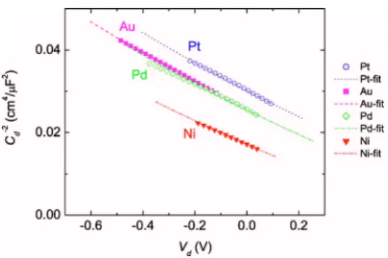
Figure4shows that the 1/C2-V curves for our junctions are almost linear under the low voltage reverse bias region. Large current under the large bias region hinders reliable
C-V measurements. Conventional Schottky junctions at the
reverse bias region have the following relationship: 1/C2=共V
bi− V − kBT/q兲/qSND, 共3兲
where Vbi is the built-in potential, and S and ND are the
dielectric constant and the donor concentration of Nb:STO, respectively. Vbi andSNDcan be extracted from the
inter-section and slope of the straight lines fitted to the experimen-tal data, as shown in Fig. 4. Such analyses reveal several extraordinary facts. First, the slope of the 1/C2-V curve
共pro-portional to 1/SND兲 is different for each electrode. All of the
electrodes were deposited on the same Nb:STO sample in our study, soSNDshould be the same. Second, the
extrapo-lated C-V curves yield very large Vbi: 2.65, 2.55, and
2.06 eV for Au, Pd, and Pt, respectively. These values are much larger than B and also larger than half of the STO
band gap 共3.3 eV兲.13Yoshida et al. explained the lower ca-pacitance and higher built-in potentials of the Au/Nb:STO junctions by assuming a low dielectric constant interfacial layer.15The total junction capacitance C can be written in the following form:
1/C = 1/Ci+ 1/Cd, 共4兲
where Ciand Cdare the capacitances of the interfacial layer
and the depletion layer, respectively. The total applied volt-age V also can be written as
V = Vi+ Vd, 共5兲
where Vi and Vd are the voltages applied to the interfacial
layer and the depletion layer, respectively.
As noted in Fig. 4, the 1/C2-V curves deviate slightly
from a straight line. This slight nonlinear behavior may be caused by the electric field dependent permittivity S of
STO: S= b/共a+E2兲1/2 共a=1.64⫻1015V2/m2 and b = 1.42
⫻1010V2/m2兲.15–18
Hikita et al. derived the junction capaci-tance as
1/Cd 2
= 2
冑
a共Vbi− Vd− kBT/q兲共bq0ND兲+共Vbi− Vd− kBT/q兲2/共b0兲2, 共6兲
where 0 is the vacuum permittivity and ND is the doping
concentration 共2.3⫻1019cm−3兲.18
The C-V data can be ana-lyzed using Eqs. 共4兲–共6兲, and properly chosen Ci and Vbi
values can reproduce the experimental data shown in Fig.4. The estimated Vbi values 共0.8–1.2 eV兲 are close to the B
values. The Ci value for our Au/Nb:STO junction 共6.2
⫻10−6 F/cm2兲 is also comparable to the value reported by
Yoshida et al. 共9.5⫻10−6F/cm2兲.15
In addition, the ⌬B
=共B,HRS−B,LRS兲 and ⌬Vbi=共Vbi,HRS− Vbi,LRS兲 values are similar. All of these results suggest that the model used in our analyses is appropriate.
Figure5共a兲shows n and Cifor the junctions: the
junc-tions with larger Civalues have smaller n values. This
mani-fests the presence of the interface layer of our junctions. Since part of the bias voltage is dropped across the insulating interface layer, the barrier height should depend on the bias voltage. The interface layer thickness␦i is related to Ci
ac-cording to the relation Ci=i/␦i. Thus, an increase of␦i共i.e.,
decrease of Ci兲 will raise n.16
Figure5共b兲shows the extractedBand Vbifor the HRS
of our junctions. Vbiis larger than Bby about 0.1共0.4兲 eV
for the Ni, Au, and Pd 共Pt兲 electrodes. In an ideal junction, the difference Vbi−B corresponds to the depth of the Fermi
level below the conduction band minimum. In Nb:STO, this difference is about 0.1 eV,18 which is comparable to the re-sults for the Ni, Au, and Pd electrodes. In real junctions, any nonhomogeneity at the interface can alter the local barrier height, and defects may act as intermediate states for trap-assisted tunnel currents.20 Either of these anomalies can
FIG. 3. 共Color online兲 1/C2-V curves of the M/Nb:STO junctions with
various electrodes.
FIG. 4. 共Color online兲 1/Cd2-Vd curves of the M/Nb:STO junctions with
various electrodes. The symbols and dotted lines indicate the experimental data and fitting results, respectively.
lower B in the I-V characteristics. C-V measurements are
less prone to such local fluctuation since the barrier height with the largest contact area dominates the C-V behavior. Therefore, the large Vbi−B value for the Pt junction
indi-cates that the barrier height fluctuation and/or trap-mediated conduction can be significant.
Figure 5共b兲 clearly shows that the resistance switching ratio, 共RHRS− RLRS兲/RHRS, has a tendency similar to that of Vbi.共No clear relationship can be found between the
inter-face capacitance and the resistance switching ratio.兲 To ex-plain such trends, a possible mechanism can be proposed as follows. First, a large barrier height will increase the maxi-mum electric field 共Emax兲 in the depletion region, Emax
=关2qND共Vbi− V − kBT/q兲/S兴1/2.20 The electric field can
pro-mote the charge trapping/detrapping in the interface states9 and/or oxygen vacancy migration.10Second, interfacial reac-tions such as the oxidation of metals and metal encapsulation can be enhanced under a large electric field at the interface.21 Either of these mechanisms can alter the barrier height and the junction resistance.
Interfacial reaction effects on the transport are evident from the Ni/Nb:STO junction results. It possesses a smaller barrier height compared with those of the noble metal 共Pd, Au, and Pt兲/Nb:STO junctions. The Ni/Nb:STO junction has the smallest VbiandB, and the largest Ci. This supports
the idea that the reaction 共oxidation兲 occurs at the Ni/Nb:STO interface, resulting in the lowering of the barrier height and the reduction of the interface layer thickness. Moreover, the hysteretic I-V behavior disappeared after an-nealing the Ni/Nb:STO junctions at 300 °C for 30 min. 共All of the other junctions with Pd, Au, and Pt still exhibited the hysteresis after the same heat treatment.兲 These results sug-gest that interfacial oxygen vacancy concentration may be involved in the interface state formation and the related re-sistance switching behaviors of our junctions.
IV. CONCLUSIONS
The rectifying metal/Nb:STO junctions formed with high work function metal electrodes 共Ni, Pd, Au, and Pt兲 exhibited hysteretic I-V and C-V characteristics. Junction pa-rameters, such as barrier heights, built-in potentials, ideality factors, and interface layer capacitance, were extracted from analyses of the electrical properties. The barrier height, pre-dicted from the Schottky–Mott rule, was largely different from the estimated results. The presence of the interface states and insulating interface layers was also noticed. The relationship between the junction parameters and the resis-tance switching ratio was examined: the junction with larger built-in potential showed larger resistance switching ratio. The resistance switching ratio did not show explicit depen-dence on the other junction parameters. The interface states, presumably related to oxygen vacancies, seemed to play cru-cial roles in the resistance switching behaviors at the metal/ Nb:STO interface.
ACKNOWLEDGMENTS
This work was supported by the Korea Research Foun-dation Grant funded by the Korean Government共MOEHRD兲 共KRF-2007-331-C00083兲.
1S. Seo, M. J. Lee, D. H. Seo, E. J. Jeoung, D.-S. Suh, Y. S. Joung, I. K.
Yoo, I. R. Hwang, S. H. Kim, I. S. Byun, J.-S. Kim, J. S. Choi, and B. H. Park,Appl. Phys. Lett.85, 5655共2004兲.
2K. M. Kim, B. J. Choi, Y. C. Shin, S. Choi, and C. S. Hwang,Appl. Phys.
Lett.91, 012907共2007兲.
3A. Chen, S. Haddad, Y. C. Wu, Z. Lan, T. N. Gang, and S. Kaza,Appl.
Phys. Lett.91, 123517共2007兲.
4M. J. Rozenberg, I. H. Inoue, and M. J. Sánchez, Phys. Rev. Lett.92,
178302共2004兲.
5D. Choi, D. Lee, H. Sim, M. Chang, and H. Hwang,Appl. Phys. Lett.88,
082904共2006兲.
6K. Szot, W. Speier, G. Bihlmayer, and R. Waser, Nat. Mater. 5, 312
共2006兲.
7T. Fujii, M. Kawasaki, A. Sawa, Y. Kawazoe, H. Akoh, and Y. Tokura,
Phys. Rev. B75, 165101共2007兲.
8S. H. Jeon, B. H. Park, J. Lee, B. Lee, and S. Han,Appl. Phys. Lett.89,
042904共2006兲.
9A. Sawa, T. Fujii, M. Kawasaki, and Y. Tokura,Appl. Phys. Lett.85, 4073
共2004兲.
10K. Tsubouchi, I. Ohkubo, H. Kumigashira, M. Oshima, Y. Matsumoto, K.
Itaka, T. Ohnishi, M. Lippmaa, and H. Koinuma,Adv. Mater.共Weinheim, Ger.兲19, 1711共2007兲.
11H.-S. Lee, J. A. Bain, S. Choi, and P. A. Salvador,Appl. Phys. Lett.90,
202107共2007兲.
12Y. Tokunaga, Y. Kaneko, J. P. He, T. Arima, A. Sawa, T. Fujii, M.
Ka-wasaki, and Y. Tokura,Appl. Phys. Lett.88, 223507共2006兲. 13J. Robertson,J. Vac. Sci. Technol. B18, 1785共2000兲.
14W. Ramadan, S. B. Ogale, S. Dhar, L. F. Fu, S. R. Shinde, D. C.
Kun-daliya, M. S. R. Rao, N. D. Browning, and T. Venkatesan,Phys. Rev. B
72, 205333共2005兲.
15A. Yoshida, H. Tamura, K. Gotoh, H. Takauchi, and S. Hasuo,J. Appl.
Phys.70, 4976共1991兲.
16S. Suzuki, T. Yamamoto, H. Suzuki, K. Kawaguchi, K. Takahashi, and Y.
Yoshisato,J. Appl. Phys.81, 6830共1997兲.
17T. Shimizu and H. Okushi,J. Appl. Phys.85, 7244共1999兲.
18Y. Hikita, Y. Kozuka, T. Susaki, H. Takagi, and H. Y. Hwang,Appl. Phys.
Lett.90, 143507共2007兲.
19R. A. van der Berg, P. W. Blom, J. F. M. Cillessen, and R. M. Wolf,Appl.
Phys. Lett.66, 697共1995兲.
20S. M. Sze and K. K. Ng, Physics of Semiconductor Devices, 3rd ed.
共Wiley, Hoboken, 2007兲.
21Q. Fu and T. Wagner, J. Phys. Chem. B 109, 11697共2005兲.
FIG. 5.共Color online兲 共a兲 The junction parameters 共n and Ci兲 and 共b兲 barrier
height共Band Vbi兲 for the HRS and the resistance switching ratio of the
M/Nb:STO junctions with various electrodes.