P1-2 / C. H. Park
IMID 2009 DIGEST •
Abstract
We report on the fabrication of ZnO-based dual gate (DG) thin-film transistors (TFTs) with 20 nm-thick Al2O3 for both
top and bottom dielectrics, which were deposited by atomic layer deposition on glass substrates at 200 oC. Whether top or bottom gate is biased for sweep, our TFT almost symmetrically operates under a low voltage of 5 V showing a field mobility of ~0.4 cm2/V·s along with the on/off ratio of 5x10⁴. The threshold voltage of our DG TFT was systematically controlled from 0.5 to 2.0 V by varying counter gate input from +5 to -2 V.
1. Introduction
ZnO-based thin-film transistors (TFTs) and their integration on glass substrate have been extensively studied with many efforts to achieve the driver or peripheral circuit components of next generation display [1-4]. Although several researchers have made progresses in performance of ZnO-based TFTs, major issues on ZnO-based circuits still remain: low voltage devices for logic and peripheral circuits, threshold voltage (Vth) control for logic inverter, gate stability
and ambient-dependent stability of ZnO TFTs. In recent years, a few low voltage ZnO-TFTs have been reported and their logic application was seen [5-6].
The reports on Vth control in ZnO devices are also
found but are rare yet. Park et al shows the feasibility of controlling of Vth by adjusting the thickness of
active layer due to change of contact resistance [7],
but their approach is still far from practical use. Our previous approach was to inject free charges into the middle of triple nanometer-thick dielectric layer by using high voltage gate bias but the process is quite complicated [8]. Dual gate (DG) TFT is another way
to control the Vth, independently utilizing top and
bottom gate of the device. Organic TFT researchers already approached to this dual gate technique [9-10].
However, ZnO-based TFT has not adopted this dual gate method but only one very recent study, where quite high voltages were applied onto DG ZnO-based TFT with two different dielectrics to observe and understand device property changes [11]. In this letter, we adopted the DG method for our low voltage ZnO-TFTs to control the Vth of TFTs or to control the
transition voltage of ZnO-based load resistive-inverter by using identically thin top and bottom gate dielectrics of Al2O3. Our DG-TFTs showed good Vth
control and good electrical stability as well. We further believe that our DG TFT may even keep ambient-dependent stability due to its self-encapsulation by top Al2O3 dielectric.
2. Experimental
Our ZnO DG-TFTs were fabricated with patterned chromium (Cr) bottom gate electrode on glass. The width of Cr electrode was 250 μm with the thickness of 150 nm. As a bottom dielectric, a 20 nm-thick Al2O3 layer was deposited on the patterned Cr by
atomic layer deposition (ALD) at a temperature of 200
oC. After dielectric substrate cleaning, 60 nm-thick
ZnO channels were deposited at room temperature (RT) by 100 W rf magnetron sputtering of ZnO targets (99.999 %) in the 10 mtorr Ar/O2 (6:1) gas
mixture, through a shadow mask for patterning (area = 500x500 μm2). Aluminum (Al) source/drain (S/D)
electrodes were subsequently deposited by thermal evaporation. The nominal channel length (L) was 90
Threshold voltage control in dual gate ZnO-based thin film
transistors
Chan Ho Park
1, Kimoon Lee
1, Kwang H. Lee
1, Byoung H. Lee
2, Myung M.
Sung
2and Seongil Im
1*1 Institute of Physics and Applied Physics, Yonsei University, Seoul 120-749, Korea
Tel.:82-2-2123-4928, E-mail: [email protected]
2 Department of Chemistry, Hanyang University, Seoul 133-791, Korea
P1-2 / C. H. Park
• IMID 2009 DIGEST
μm and the width (W) was 500 μm. Until this step, the bottom part of ZnO DG-TFT was formed. Next, as a top gate dielectric, another 20 nm-thick Al2O3 layer
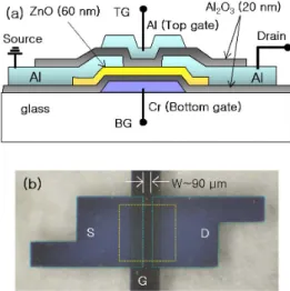
was deposited by ALD with the same condition taken for the bottom dielectric deposition. To form the top gate electrode, a patterned 150 nm-thick and 250 μm-wide Al (which is known to have a similar work function to that of Cr[12]) was evaporated onto the top of gate dielectric. Figures 1(a) and 1(b) show the schematic cross-sectional and photographic plan views of our dual gate device. After that, the dielectric layers were patterned by photolithography and wet etching to open S/D and bottom gate contact. All the electrical properties of our devices were measured by a semiconductor parameter analyzer (HP4155C, Agilent Technologies). The capacitance-voltage (C-V) measurements at 1 MHz of the Al2O3 dielectric layer
were measured with an LCR meter (HP4284A, Agilent Technologies), adopting 250 μm-diameter Al dot/dielectric/Cr structure. Our 20 nm-thick ALD-grown Al2O3 displays capacitance of 320 and 285
nF/cm2 in bottom and top dielectric layer, respectively
(dielectric constant ~ 7.2 and 6.5) and shows a good dielectric strength of higher than 3 MV/cm.
3. Results and discussion
Figure 2(a) shows the drain current-drain voltage curves (ID-VD) obtained from the top gate (TG)-swept
top channel and the bottom gate (BG)-swept bottom channel (the top and bottom electrode has alternately been grounded during each operation). At a low gate voltage of 5 V, the saturation current was observed to be 1.0 and 1.4 μA for the top and bottom channel, respectively. In comparison with TG-controlling TFTs, BG operation always displayed slightly higher drain current than that of TG-sweeping device.
Figure 2(b) shows the transfer curves (square root of drain current-gate voltage (√ID-VG) and log10(ID
)-VG curves) obtained from the TG- and BG-swept
channels. Gate leakage current was less than 200 pA for all the TFTs (data not shown here). The field effect (saturation) mobility from top channel was estimated to be ~0.3 cm2/V⋅s with a threshold voltage (V
th) of
1.62 V while the on/off current ratio was 5.5x10⁴
along with a sub-threshold slope of 0.53 V/dec. Here, the field effect mobility of DG-TFTs may not be simple to estimate even with their transfer curves. It is because the channel formation of DG-TFTs, where one gate electrode is grounded, is affected by the bottom dielectric capacitor as well as the top capacitor,
unlike the case of conventional TFT with a single gate electrode [9, 11]. Therefore, the effective dielectric capacitance for DG-TFT, where the top- and bottom-gate electrodes are independently controlled, should be calculated as follows, considering serially connected capacitors but excluding any parasitic capacitance term of depleted ZnO thickness from calculation, (where for a precise estimation of Ctotal the
parasitic capacitance term is necessary but is difficult to know here): bottom top total C C C 1 1 1 = + (1),
where Ctop and Cbottom are the capacitance of top and
bottom dielectric layers, and Ctotal is the effective
value of serially-connected double dielectrics. From above equation (1), we calculated Ctotal value as 151
nF/cm2, which is about a half of dielectric
capacitances (Ctop ~285 nF/cm2 and Cbottom ~320
nF/cm2). By using the same C
total as used for top
channel TFT, the field effect (saturation) mobility of bottom channel was estimated to be ~0.47 cm2/V⋅s
which is a little higher than that of top channel (~0.3 cm2/V⋅s). (Of course the top channel and bottom
channel mobilities should be higher than above values if further considering the parasitic capacitances from ZnO depletion.) Bottom channel TFT showed the threshold voltage (Vth) of 1.62 V and on/off current
ratio of 5.0x10⁴ and along with a sub-threshold slope
of 0.47 V/dec which are very similar to those from the top channel. Therefore, based on the results in Figure 2(a) and 2(b), the top and bottom channels of our DG-TFT show almost symmetric behavior in operation.
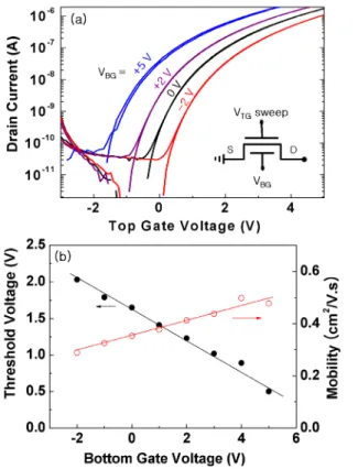
Figure 3(a) shows the transfer characteristics of top channel in our DG-TFT under the variation of BG voltage (VBG) from -2 to +5 V. First of all, the transfer
curves show that our ZnO TFTs are electrically stable with very little gate-hysteresis. As the next but main point, Figure 3(a) displays that our top gate ZnO-TFT has a shift of transfer curve or shift of Vth with respect
to the VBG variation, which is similar to the body bias
effects observed in Si-based field effect transistors. A positive VBG induces a smaller Vth than the original Vth
(VBG= 0 V) while a negative VBG works in the
opposite way. The results of such Vth shift with respect
to VBG variation appear quite systematic as plotted in
Figure 3(b); with the VBG varied from -2 to +5 V, the
Vth changes from 2 to 0.5 V. These changes can be
estimated with back-gate effect factor (
γ
) which was addressed in the potential model of dual gate fieldP1-2 / C. H. Park
IMID 2009 DIGEST •
effect transistor with an identical capacitance for the top and bottom insulators as follows[13],
ZnO dielec dielec ZnO dielec ZnO Back th
t
k
t
k
t
k
V
V
⋅
+
⋅
⋅
−
=
Δ
=
γ
(2)where VBack is now VBG, kZnO and kdielec are the
dielectric constant of active ZnO layer and dielectric (Al2O3) layer, and tZnO and tdielec are the thickness of
active ZnO layer and dielectric layer, respectively. The negative sign in equation (2) means that the changing direction of Vth is opposite to that of the VBG in our
device. The plotted Vth change in Figure 3(b) provides
γ = -0.27 while the equation (2) does quite a close value range of γ = -0.25 ~ -0.36. (Here, adequate dielectric constant values of kZnO = 7~11 and kdielec =
6.5~7.2, were used as obtained from C-V measurement (~10) and literature [14-15].) According to the Figure 3(b), the saturation mobility was also systematically changed with the VBG but the change
was quite minor (from 0.3 to 0.47 cm2/V s).
Figure 4 shows the static behavior of the resistive-load inverter using a circuit combining 22 M Ω load resistor and our DG-TFT, where input voltage (Vin) was provided from top gate under a certain VBG
(=+5, +2, 0, and -2 V) and a supply voltage (VDD= 5
V). A schematic inverter circuit is displayed in the inset. From these experiments, we obtained four voltage transfer curves (VTC) with respect to each VBG, and also achieved the maximum VTC voltage
shift of ~1.5 V in the present VBG range (of +5 ~ -2 V).
It is interesting to note that the VTC shift window (1.5 V) is the same as the amount of Vth shift (from 0.5 to
2 V as shown in Figure 3(b)). It means that our ZnO-based DG-TFT can somewhat flexibly control the VTC characteristics by selectively biasing either top or bottom gate. The output voltage gain (Vout/Vin) was
~4.5 for all the inverters.
Fig. 1. (a) Schematic cross-sectional view and (b) photographic plan view of DG-structured ZnO TFT.
Fig. 2. (a) The drain current-drain voltage curves (ID-VD) and (b) the
transfer curves (square root of drain current-gate voltage (√ID-VG)
and log10(ID)-VG curves)obtained from the top gate (TG)-swept top
channel and the bottom gate (BG)-swept bottom channel (the top and bottom electrode has alternately been grounded during each operation).
P1-2 / C. H. Park
• IMID 2009 DIGEST
Fig. 3 (a) The transfer characteristics of top channel in our DG-TFT obtained under varied VBG. (b) The plots of VBG vs. Vth and of VBG vs.
saturation mobility as obtained from the TG-swept ZnO-TFT under varied VBG.
Fig. 4. The static behavior of the resistive-load inverter using a circuit combining 22 MΩ load resistor and our DG-TFT, where the voltage of bottom gate (VBG) changed from -2 to +5 V at a 5 V supply voltage
(VDD).
4. Summary
In the present work, we focus on the device physics of dual gate (DG) ZnO-based thin-film transistors (TFTs) with two channels at top and bottom of ZnO layer that is sandwiched by thin Al2O3
dielectrics. This dual gate structure is promising to control threshold voltage of device as a very new
study in ZnO TFT field. We hope that our work may provide good information to researchers of oxide semiconductor.
Acknowledgement
The authors acknowledge the financial support from the fundamental R&D Program for Core Technology of Materials funded by the Ministry of Knowledge Economy, the IT R&D program of MKE/IITA [2006-S079-02, Smart window with transparent electronic devices], the Korea Science and Engineering Foundation (KOSEF) grant funded by the Korea government (MEST) (No. 2009-8-0430) and Brain Korea 21 Program. C. H. Park thanks for the Seoul Science Fellowship. The authors would like to thank Byoung H. Lee and prof. Myung M. Sung for support in fabrication process.
5. References
1. E. Fortunato, P. Barquinha, A. Pimentel, A. Goncalves, A. Marques, L. Pereira, and R. Martins, Adv. Mater., Vol. 17, p.590 (2005).
2. J. F. Wagner, Science, Vol. 300, p.1245 (2003).
3. K. Nomura, H. Ohta, A. Takagi, T. Kamiya, M. Hirano, and M. Hosono, Nature, Vol.432, p.488 (2004).
4. J. Sun, D. Mourey, D. Zhao, S. K. Park, S. F. Nelson, D. H. Levy, D. Freeman, P. Cowdery-Corvan, L. Tutt, and T. N. Jackson, IEEE Electr. Dev. Lett,. Vol. 29, p.721 (2008).
5. M. S. Oh, D. K. Hwang, K. Lee, S. Yi, and S. Im, Appl. Phys.
Lett., Vol. 90, p.173511 (2007).
6. S. H. Cha, M. S. Oh, K. H. Lee, B. H. Lee, M. M. Sung, and S. Im, Appl. Phys. Lett., Vol. 92, p.023506 (2008).
7. J. S. Park, J. K. Jeong, Y. G. Mo, H. D. Kim, and C. J. Kim,
Appl. Phys. Lett., Vol. 93, p.033513 (2008).
8. S. H. Cha, M. S. Oh, K. H. Lee, J. M. Choi, B. H. Lee, M. M. Sung, and S. Im, IEEE Electr. Dev. Lett., Vol. 9, p.1145 (2008). 9. L. Chua, R. H. Friend and P. K. H. Ho, Appl. Phys. Lett., Vol. 87,
p.253512 (2005).
10. J. B. Koo, J. W. Lim, S. H. Kim, C. H. Ku, S. C. Lim, J. H. Lee, S. J. Yun, and Y. S. Yang, Electrochem. Solid-State Lett., Vol. 9, p.G320 (2006).
11. H. Lim, H. Yin, J. S. Park, I. Song, C. Kim, J. Park, S. Kim, S. W. Kim, C. B. Lee, Y. C. Kim, Y. S. Park, and D. Kang, Appl.
Phys. Lett., Vol. 93, p.063505 (2008).
12. S. J. Pearton, J. C. Zopler, R. J. Shul, and F. Ren, J. Appl.
Phys., Vol. 86, p.1 (1999).
13. J. W. Han, C. J. Kim, and Y. K. Choi, IEEE Trans. Electr. Dev,. Vol. 55, p.1472 (2008).
14. R. Menon, K. Sreenivas and V. Gupta, J. Appl. Phys,. Vol. 103, p.094903 (2008).
15. N. Ashkenov, B. N. Mbenkum, C. Bundesmann, V. Riede, M. Lorenz, D. Spemann, E. M. Kaidashev, A. Kasic, M. Schubert, M. Grundmann, G. Wagner, H. Neumann, V. Darakchieva, H. Arwin, and B. Monemar, J. Appl. Phys., Vol. 93, p.126 (2003).