P1-82 / J.-H. Kim
• IMID 2009 DIGEST
Improvement of PMOLED life time using Mg-Zn-F thin film passivation
Jae-Hyun Kim
1, Jun-Seon Seo
1, Seok-Min Hong
1, Byoung-Ho Kang
2, Do-Eok Kim
2,
Sung-Youp Lee
3, Byong-Wook Shin
4, Hyeong-Rag Lee
4,Hak-Rin Kim
2and Shin-Won Kang
2,†1Department of Sensor and Display Engineering, Kyungpook National Univ., Deagu, Republic of Korea Tel: 82-53-940-8609, E-mail: [email protected]
2,†School of Electrical Engineering and Computer Science, Kyungpook National Univ., Daegu, Korea 3Department of Nano-Science & Technology, Kyungpook National Univ., Daegu, Korea
4Department of Physics, Kyungpook National Univ., Daegu, Korea
Keywords : thin film passivation, life time, pmoled
Abstract
We manufactured a novel gas permeation thin film passivation by using inorganic Mg-Zn-F target which has better optical characteristics and high electronegativity. We fabricated targets in various composition ratio and formed about 200nm which is limited thickness of the flexible display. Applied to
PLED device, the target which composed of MgF2
and Zn at the ratio of 4:6, WVTR was reached the measurement limit of the equipment, 10-3g/m2·day and the life time was increased 25 times better than PLED device which is non-passivation.
1. Introduction
Recently, rapid technology development and wide range of spread of information technology caused increasing demand for handsets which have a small sized mobile display. This trend requires a lightweight, thin and low power consumption. Organic light emitting diodes (OLED) have come into the spotlight with the next generation display which acceptable those demands among the various kinds of displays.
OLED have many merits, such as high brightness, fast response characteristics, wide visible angles and simple manufacture process more than LCD and PDP. Significant benefit of OLED displays over traditional liquid crystal displays (LCD) is that OLED do not require a backlight to function. Because there is no need for a backlight, an OLED display can be much thinner than an LCD panel 1.
However, the biggest technical problem for OLED is the limited life time of the organic materials.
Moisture and oxygen caused oxidation of the organic material that means the device should be protected from moisture and oxygen. Consequently, OLED is necessary to passivation which interrupts moisture and oxygen, and if exposed, black spots and LED shrinks, which will reduce the life time of the display devices 2-5.
In this study, we have manufactured Mg-Zn-F thin film using target mixed various ratio of MgF2 to Zn
for thin film encapsulation using radio frequency (RF) magnetron sputtering. Considering the gas permeation mechanism, the sputtering method that can deposit boundary parts between islands as lattice defect or nano defect was used to increase the packing density. Manufactured thin film passivation Water Vapor Transmission Rate (WVTR) was equal to or less than 10-3g/m2·day. Thin film composition
and gas permeation characteristics were evaluated, and the possibility as a new passivation technology was confirmed. Also it applied to polymer OLED device, improved life time.
2. Experimental
In this study, we fabricated targets for sputtering by mixing MgF2 and Zn after heating each of them
above the melting point, to create thin films where MgF2 and Zn are physically mixed in an amorphous
structure.
Targets were fabricated in various composition ratios by varying the mix ratio of MgF2 and Zn to
3:7, 4:6 and 5:5 to observe the variation of the Zn ratio by the composition of ratio of MgF2 and Zn. A
P1-82 / J.-H. Kim
IMID 2009 DIGEST • using an RF magnetron sputter. We have
manufactured thin film which composed 4 layers on glass substrate in order to confirm properties of passivation.
Fig. 1. Schematic diagram of PLED element deposited with passivation film.
In figure 1, the device manufactured 4 layers which consist of anode, hole injection layer (HIL), emission layer(EML) and cathode to evaluate LED device. Indium tin oxide (ITO) was used for anode patterned by photolithography process and deposited on glass to a thickness of 1,500 Å. Then, we formed a HIL about 25 nm
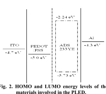
thickness using PEDOT:PSS (poly(ethylenedioxythiophene): polystyrene sulphonate, Baytron P AI 4083, H. C. Starck) on
ITO. It was used as the buffer layer on the anode mainly to increase the anode work function from 4.7 eV to 5.0 eV and to reduce the surface roughness of the anode to obtain stable and pin-hole-free electrical conduction across the device. Emission layer (poly[9,9-dioctylfluorenyl-2,7-diyl)-co-1,4-benzo-{2,1’-3}-thiadiazole)], ADS 233YE) dissolved in the toluene and formed EML on HIL by spin coating. The Al metal layer for cathode which intersected with anode by thermal evaporation with shadow mask was deposited on EML
The energy levels of the materials involved in the PLED are shown in Figure 2.
Fig. 2. HOMO and LUMO energy levels of the materials involved in the PLED.
We manufactured the targets which were made of MgF2 and Zn in order to evaluate the gas permeation
status of an OLED glass substrate which has better optical characteristics and high electronegativity with various ratios. Zn atoms were deposited with MgF2, they are inserted into the molecular lattice and
fixed at neutral points. This will increase the packing density and electronegativity of the molecule and prevent the permeation of moisture and oxygen, effectively 6,7. We produced targets with various
ratio of MgF2 to Zn (5 : 5, 4 : 6 and 3 : 7) to control
the amount of Zn in the passivation film,. Mg-Zn-F films were deposited on glass substrate using RF magnetron sputterby the conditions in table 1. Table 1. Sputtering conditions used to fabricate Mg-Zn-F passivation film.
Parameter Condition Target - substrate distance
Sputtering pressure Gas flow rate
RF power Deposition rate 11 cm 4.7 × 10⁻⁵ Torr 50 sccm 100 W 0.1 nm / min
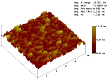
We confirmed eligible to use passivation film through surface morphology and thickness of the thin film was measured by SEM and AFM. Figure 3,4 shows an SEM and AFM image of Mg-Zn-F single thin film, respectively.
P1-82 / J.-H. Kim
• IMID 2009 DIGEST
Fig. 3. SEM image of Mg-Zn-F passivation film.
Fig. 4. AFM image of Mg-Zn-F passivation film.
3. Results & Discussion
Target which composed of MgF2 and Zn at the
ratio of 4:6 reached the WVTR measurement limit of the equipment, 10-3g/m2·day when increase of the Zn portion in thin film in figure 5.
Fig. 5. WVTR and Zn portion data of Mg-Zn-F thin film passivation deposited at 200 ㎚ thickness. In order to confirm the passivation films, we made PLED device. Turn-on voltage of the device was 5.5 V, maximum luminance was about 8,200 cd/m2 and
efficiency was 1.2 cd/A. As a result in figure 5, we made a device with passivation film which has 4:6 target according to lowest WVTR. We confirmed life time of non-passivation film device was 800 sec at the half of the max luminance but the passivation film device was 20,000 sec at the same condition. Therefore passivation film which has lowest WVTR device can be prevented moisture and oxygen more effectively and improved life time 25 times better than non-passivation device.
4.
Summary
We manufactured a novel gas permeation thin film passivation by using inorganic Mg-Zn-F. Passivation film was formed about 200 nm that is limited thickness of the flexible display. Applied to PLED device, life time was increased 25 times better than PLED device which is non-passivation.
Acknowledgement
This research was financially supported by the Ministry of Education, Science Technology (MEST) and Korea Institute for Advancement of Technology(KIAT) through the Human Resource Training Project for Regional Innovation
5. References
1. B. A. MacDonald, K. Rollins, D. MacKerron, K. Rakos,R. Eveson, K. Hashimoto and B. Rustin,
P1-82 / J.-H. Kim
IMID 2009 DIGEST •
Flexible Flat Panel Displays, p. 1 (2005).
2. S. M. Cho, M. H. Oh, S. H. Lee and D. J. Choo,
J.Korean Phys. Soc., Vol. 48, S107 (2006).
3. H. Tang, L. Zhu, Y. Harima and K. Yamashita,
Synt.Mater, Vol. 110, p.105 (2000).
4. V. Tsakova, S. Winkels and J. W. Schultze,
Electrochimica Acta, Vol. 46, p.759 (2000).
5. L. M. Do, E. Han, Y. Niidome, M. Fujihira, T. Kanno,S. Yoshida, A. Maeda and A. J. Ikushima,
J. Appl. Phys, Vol. 76, p.5118 (1994).
6. Do-Eok Kim, Byoung-Ho Kang, Su-Hwan Kim, Seok-Min Hong, Sung-Youp Lee, Byong-Wook Shin, Hyeong-Rag Lee, Dae-Hyuk Kwon and Shin-Won Kang, J. Korean Phys. Soc., Vol. 54, p. 231~235 (2009).
7. M.Yano and K.Inaba, Journal of Crystal