Vol. 18, No. 6, pp. 323-329, December 25, 2017
323 http://www.transeem.org
Regular Paper
OAK Central: http://central.oak.go.kr
DOI: https://doi.org/10.4313/TEEM.2017.18.6.323
pISSN: 1229-7607 eISSN: 2092-7592
† Author to whom all correspondence should be addressed:
E-mail: [email protected]
Copyright ©2017 KIEEME. All rights reserved.
This is an open-access article distributed under the terms of the Creative Commons Attribution Non-Commercial License (http://creativecommons.org/licenses/by-nc/3.0) which permits unrestricted noncommercial use, distribution, and reproduction in any medium, provided the original work is properly cited.
Effect of Double Schottky Barrier in Gallium-Zinc-Oxide
Thin Film
Teresa Oh
†Department of Semiconductor Engineering, Cheongju University, Cheongju 28503, Korea
Received August 14, 2017; Received September 10, 2017; Accepted September 12, 2017
This reports the electrical behavior, bonding structure and Schottky contact of gallium-zinc-oxide (GZO) thin film annealed at 100~400℃. The mobility of GZO with high density of PL spectra and crystal structure was also increased because of the structural matching between GZO and Si substrate of a crystal structure. However, the GZO annealed at 200℃ with an amorphous structure had the highest mobility as a result of a band to band tunneling effect. The mobility of GZO treated at low annealing temperatures under 200℃ increased at the GZO with an amorphous structure, but that at high temperatures over 200℃ also increased when it was the GZO of a crystal structure. The mobility of GZO with a Schottky barrier (SB) was mostly increased because of the effect of surface currents as well as the additional internal potential difference.
Keywords : GZO, PL spectra, Schottky barrier, XPS, Tunneling
1. INTRODUCTION
The Zn based oxide semiconductor has been researched as prom-ising transparent electrode materials instead of ITO to have possi-bility of flexipossi-bility and low price. The ZnO is developed with doping materials of Al, Ga, Ag, Ge, Sn to overcome the humidity in an air condition [1-4]. The oxide semiconductor was generally improved by annealing processes to increase the mobility and stability, because the oxygen vacancy as charge carriers was formed by the annealing and moreover the chemical mechanical properties also improved. The high mobility transistor was made by the trapping phenomenon based on the Ohmic contact, and proportioned to the amount of doping carriers. However, the reduction of size of device limited the doping carrier in the channel layer [5-9]. Therefore, the transistor has the problem of degradation of mobility and stability. Recently, many researchers have focused on the transistor with a tunneling effect to increase the mobility and improve the threshold voltage shift. The transistor with the tunneling phenomenon was operated by the
ambipolar transfer characteristics in a depletion layer [10-12]. The diffusion current is the opposite direction current due to the poten-tial barrier and the band to band conduction of diffusion current in a depletion region is the same effect of the tunneling phenomenon as the Schottky conduction. So the mobility abruptly increases.
This study was researched the correlation between the crystal structure and electrical properties of oxygen semiconductor. The ZTO films were annealed with various temperatures to research the physical-electrical characteristics of ZTO. It was researched the correlation between electrical properties and the contact mechanism in according to the crystal and amorphous structures, moreover the difference between the drift current and diffusion current was observed.
The analysis of electronic characteristic becomes more importance with decreasing the device size. Reduction in a size emphases the effect of depletion layer in a thin film transistor [1-5]. Development of these new materials requires greater understanding and control of their electronic contacts. For the understanding of how electronic properties depend on the nature of surfaces of oxide semiconductor, many groups have investigated the influences of defects for the trapping in a channel and the tunneling effect of depletion layer to solve the electrical unstability of oxide semiconductor TFTs [6-9]. Results involving tunneling and trapping phenomenon in oxide semiconductor through thin MOS structure had been often considered by a contact mechanism. There is a difference between
the trapping and tunneling, because the trapping is the transition by a localized trap state to conduction band in spite of the band to band transition in a tunneling. In the case of MOS structures, the process of trapping into the band to band introduces the dependence on voltage as well as oxide thickness [10,11]. The properties of the interface and the potential barrier in metal-oxide-semiconductor depended on the defect formation such as oxygen vacancies, zinc interstitials [12]. The trap states may have results from the creation of intrinsic defects and the loosely bound atom strength such as oxygen ions (O2-), oxygen vacancies (V
O2+), zinc ions (Zn+), zinc
vacancies (VZn-) and zinc interstitials (Zni) [13,14]. These defect is
affected the bonding structure of oxide semiconductors. The oxygen vacancy as carriers not only enhanced the conductivity, but also became a SB as an exhausted layer. The depletion layer plays a role in determining the contact resistance or Schottky barrier (SB) [15-18]. Therefore, the control of depletion layers had been expected to be a key factor for evaluation of a MOS or MIS contact structure [19]. It was demonstrated the relationship between the oxygen vacancy and crystallinity to increases the mobility using a Schottky barrier in gallium-zinc-oxide thin film to research the surface effect of GZO when applying an electric field. The GZO was fabricated with various oxygen flow rates and after annealed to make various type bonding structures. The analysis of GZO prepared on Si substrate was done by the XRD, PL and Hall measurement. It was studied the difference of Ohmic and Schottky contacts in accordance with the Schottky barrier.
2. EXPERIMENTS
Oxygen (99.9999%) was varied from 16 sccm to 26 sccm during the GZO deposition at 70 RF power for 10 min on a p-Si substrate. GZO targets (Ga:Zn:O=1:1:1:1, at%) were supplied by Nano Technology, Inc., Korea. The target to substrate distance was kept at 100 mm and the base pressure was 4.5 ×10⁻⁵ Torr and the working pressure of the
chamber with argon gas was 1.2~1.4 ×10⁻³ Torr. As deposited IGZO
films about 50~100 nm were annealed at 100~400℃ in the low
pres-sure condition, respectively. The physical-chemical properties were measured by X-ray diffraction pattern (Bruker AXS, D8 Discover with GADDS) and X-ray photoelectron spectroscopy (VG Science, ESCALAB 210). The photo luminance (LASER RAMAN SPECTROM-ETER) analyzed the optical characteristics of GZO. The PL spectra give the information about the exciton, electron and localized trap carriers. The relative content of oxygen vacancy was analyzed by O 1s spectra in XPS spectra, and the mobility was researched by the Hall measurement system. The electrical characteristics of IGZO films were measured by the HP4155 to research the Schottky contact and Schottky barrier.
3. RESULTS AND DISCUSSION
To research the relationship between the bonding structure and optical characteristics of oxide semiconductor, GZO thin films were deposited with various oxygen gas flows and then annealed at various temperatures.
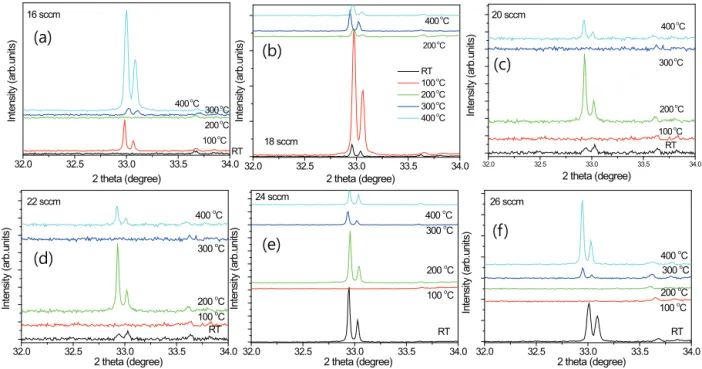
Figure 1 is the X-ray diffraction pattern of GZO annealed at various temperatures. The peak of 33o (degree) on GZO means the crystal
structural, and no signal at 33o (degree) means the amorphous
structure. The intensity of the peak at 33o (degree) changed depending
on the oxygen gas flow rates as well as annealing temperatures. Most GZO samples deposited using oxygen gas flow of 18 sccm showed the crystal structure in spite of changing the annealing temperature. But other samples with 16 sccm, 20 sccm, 22 sccm, 24 sccm and 26 sccm partially became amorphous structures with increasing the annealing temperatures. The conductivity of GZO as one of oxide semiconductors depends on oxygen vacancy (Vo+),
and the annealing in an atmosphere condition instead of a vacuum is able to make more content of oxygen vacancies. To research the relationship between the Schottky contact and conductivity of GZO, the electrical properties of GZO deposited by O2 of 18 sccm
with a crystal structure were researched in accordance with various annealing temperatures as shown in Fig. 2.
Figures 2(a) and (b) showed that all samples were Schottky contact
32.0 32.5 33.0 33.5 34.0 400 oC 300 oC 200 oC 100 oC RT 16 sccm Int ens ity (ar b. uni ts ) 2 theta (degree) 32.0 32.5 33.0 33.5 34.0 26 sccm 400 oC 300 oC 200 oC 100 oC RT Int ens ity (ar b. uni ts ) 2 theta (degree) 32.0 32.5 33.0 33.5 34.0 24 sccm 400 oC 300 oC 200 oC 100 oC RT Int ens ity (ar b. uni ts ) 2 theta (degree) 32.0 32.5 33.0 33.5 34.0 22 sccm 400 oC 300 oC 200 oC 100 oC RT Int ens ity (ar b. uni ts ) 2 theta (degree) 32.0 32.5 33.0 33.5 34.0 200 oC 400 oC 18 sccm Int ens ity (ar b. uni ts ) 2 theta (degree) RT 100 oC 200 oC 300 oC 400 oC 32.0 32.5 33.0 33.5 34.0 RT 100 oC 200 oC 300 oC 400 oC 2 theta (degree) Int ens ity (ar b. uni ts ) 20 sccm
(a)
(b)
(c)
(d)
(e)
(f)
Fig. 1. X-ray diffraction pattern of annealed GZO in an atmosphere condition with various oxygen gas flow rates. (a) 16 sccm, (b) 18 sccm, (c) 20 sccm, (d)
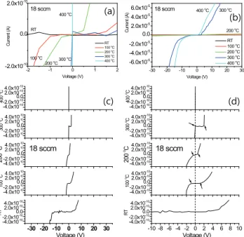
with asymmetric I-V characteristics near zero voltage. The arrow presents the Schottky contact. The current-voltage features in a range of -30 V< voltage < +30 V is not easy to define the Schottky contact. So it is need to analyze the I-V curves in a narrow range of -5 V< voltage < +5 V as shown in Fig. 2(d). Figure 2(c) shows the electrical contact properties of GZO with increasing the annealing temperature as a surface property. The current increased with increment of annealing temperatures. The non-linear Schottky contacts were observed at GZO films annealed at 100℃, 200℃ and 300℃. The GZO prepared with 18 sccm of oxygen gas flow rate have the two types of Schottky
contacts with Schottky barriers of -1 V <voltage<+1 V at both of the positive and negative voltages. The Schottky contact at GZO films annealed at 300℃ shifted to a positive voltage. The Schottky barriers at the positive and negative voltages originated from the energy banding effect due to the charge carriers trapped by the defects at the interfaces such as the GZO/Si-wafer and GZO/metal electrode. These Schottky barriers at the positive and negative voltages are the origin of ambipolar transport for the conduction in nono-scale device [9,13]. However, the GZO (18 sccm) annealed at 400℃ showed the Ohmic contact as shown in Fig. 2(c). The current-voltage characteristics of the GZO were affected by the growth of GZO. The XRD pattern of GZO (18 sccm) annealed at 400℃ has low intensity as crystal structures as shown in Fig. 1(b). Therefore, it seems does not have the trapped charge carriers such as oxygen vacancies. To research the relationship between the bonding structures and Schottky contact, the electrical properties of as deposited GZO films and annealed GZO films with various oxygen gas flow rates were observed.
Figure 3 is the correlation between XRD and electrical characteristics of GZO annealed at 100℃ with various oxygen gas flow rates. Samples with 18 sccm and 16 sccm as an oxygen gas flow rate had the Schottky contact with two kinds of SB, and the XRD pattern of theses GZO of 18 sccm and 16 sccm were shown the crystal structure as shown in Fig. 3(c). Figure 3(b) presents the GZO of 16 sccm of oxygen gas flows with low SB, and the XRD intensity was also very low. GZO films with an amorphous structure had the Ohmic contact without SB, which consists of trapped charge carriers and exhaustion layer owing to the surface effect of an energy banding. Therefore, it could be confirmed that the oxygen vacancy generated after annealing processes enhanced not only the crystallinity, but also conductivity of GZO.
Figure 5 presents the relationship between the electrical characteristics and bonding structures of GZO annealed at 300℃. The Schottky contact of GZO annealed at 300℃ was seen in the one SB at GZO of 16 sccm and 18 sccm of oxygen gas flow rates.
Figure 6 displays the electrical characteristics and bonding structures of GZO annealed at 400℃. All samples showed the various bonding structure from a crystal to amorphous structures.
-2 -1 0 1 2 -2.0x10⁻¹⁰ 0.0 2.0x10⁻¹⁰ RT 100 oC 200 oC 300 oC 400 oC 300 oC 100 oC 200 oC RT 400 oC 18 sccm Cur rent (A ) Voltage (V) (a) (b) -30 -20 -10 0 10 20 30 -4.0x10⁻¹⁰ -2.0x100.0-10 2.0x10⁻¹⁰ 4.0x10⁻¹⁰ RT -4.0x10⁻¹⁰ -2.0x100.0-10 2.0x10⁻¹⁰ 4.0x10⁻¹⁰ Voltage (V) -4.0x10⁻¹⁰ -2.0x100.0-10 2.0x10⁻¹⁰ 4.0x10⁻¹⁰ -4.0x10⁻¹⁰ -2.0x100.0-10 2.0x10⁻¹⁰ 4.0x10⁻¹⁰ -4.0x10⁻¹⁰ -2.0x100.0-10 2.0x10⁻¹⁰ 4.0x10⁻¹⁰ 18 sccm 400 oC 200 oC 100 oC 300 oC (c) -10 -8 -6 -4 -2 0 2 4 6 8 10 -4.0x10⁻¹⁰ -2.0x100.0-10 2.0x10⁻¹⁰ 4.0x10⁻¹⁰ RT -4.0x10⁻¹⁰ -2.0x100.0-10 2.0x10⁻¹⁰ 4.0x10⁻¹⁰ Voltage (V) -4.0x10⁻¹⁰ -2.0x100.0-10 2.0x10⁻¹⁰ 4.0x10⁻¹⁰ -4.0x10⁻¹⁰ -2.0x100.0-10 2.0x10⁻¹⁰ 4.0x10⁻¹⁰ -4.0x10⁻¹⁰ -2.0x100.0-10 2.0x10⁻¹⁰ 4.0x10⁻¹⁰ 18 sccm 400 oC 200 oC 100 oC 300 oC -30 -20 -10 0 10 20 30 -6.0x10⁻⁵ -4.0x10⁻⁵ -2.0x10⁻⁵ 0.0 2.0x10⁻⁵ 4.0x10⁻⁵ 6.0x10⁻⁵ 300 oC RT 100 oC 200 oC 300 oC 400 oC 200 oC 400 oC 18 sccm Cur rent (A ) Voltage (V) (d)
Fig. 2. Schottky contact and I-V characteristics of GZO with O2=18 sccm. (a)
~-10-10 A<current<~+10-10 A, (b) ~-10-5 A <current<~+10-5 A, (c) properties
of Schottky contact, and (d) of GZO annealed at 100℃, 200℃ and 300℃.
-3 -2 -1 0 1 2 3 -1.0x10⁻⁹ -5.0x10⁻¹⁰ 0.0 5.0x10⁻¹⁰ 1.0x10⁻⁹ SB 26 22 20 18 16 100 oC Voltage (V) Cu rre nt (A ) -1.0 -0.5 0.0 0.5 1.0 -1.0x10⁻¹¹ -5.0x10⁻¹² 0.0 5.0x10⁻¹² 1.0x10⁻¹¹ 24 26 22 20 18 16 100 oC Voltage (V) Cu rre nt (A ) 32.0 32.5 33.0 33.5 34.0 100 oC 26 24 22 20 18 16 Int ens ity (ar b. uni ts ) 2 theta (degree)
(a)
(b)
(c)
Fig. 3. Electrical-physical characteristics of GZO annealed at 100℃ with various oxygen gas flow rates. (a) I-V curves of GZO in accordance with the
increment of oxygen gas flow rates, (b) Schottky contact of GZO (18 sccm) obtained from I-V, and (c) XRD pattern.
-2.0 -1.5 -1.0 -0.5 0.0 0.5 1.0 1.5 2.0 -4.0x10⁻¹⁰ -2.0x10⁻¹⁰ 0.0 2.0x10⁻¹⁰ 4.0x10⁻¹⁰ SB SB 18 16 200 oC Cur rent (A ) Voltage (V) -2.0 -1.5 -1.0 -0.5 0.0 0.5 1.0 1.5 2.0 -4.0x10⁻¹⁰ -2.0x10⁻¹⁰ 0.0 2.0x10⁻¹⁰ 4.0x10⁻¹⁰ SB 22 20 16 200 oC Cur rent (A ) Voltage (V) -0.5 -0.4 -0.3 -0.2 -0.1 0.0 0.1 0.2 0.3 0.4 0.5 -4.0x10⁻¹⁰ -2.0x10⁻¹⁰ 0.0 2.0x10⁻¹⁰ 4.0x10⁻¹⁰ 26 24 16 200 oC Cur rent (A ) Voltage (V) (a) (b) (c) 32.0 32.5 33.0 33.5 34.0 Int ens ity (ar b. uni ts ) 200 oC 2 theta (degree) 26 24 22 20 18 16 (d)
Fig. 4. Electrical-physical characteristics of GZO annealed at 200℃ with various oxygen gas flow rates. (a) I-V curves of GZO with 16 sccm and 18 sccm of
oxygen gas flow rates, (b) I-V characteristics of GZO with 20 sccm and 22 sccm of oxygen gas flow rates, (c) I-V curves of GZO with 24 sccm and 26 sccm of oxygen gas flow rates, and (d) XRD pattern.
But there were no GZO films with a Schottky contact. So it could be confirmed that the annealing at 400℃ processes is not suitable for the preparing of oxide semiconductors. Because it was generally known that the Schottky contact in a semiconductor device improves the electrical properties of semiconductors.
Figure 7(a) is the O 1s spectra near the peak of 530 nm of GZO of
18 sccm were analyzed with various oxygen gas flow rates by XPS spectra, and Fig. 7(b) is the oxygen vacancy in accordance with various annealing temperatures. The oxygen vacancy was the highest at the GZO annealed at 200℃ in an air condition.
Figure 8 is the O 1s spectra near the peak of 530 nm of GZO annealed at 200℃ with various oxygen gas flow rates. The oxygen
32.0 32.5 33.0 33.5 34.0 26 24 22 20 18 16 sccm 300 oC 2 theta (degree) Int ens ity (ar b. uni ts ) -3 -2 -1 0 1 2 3 -1.0x10⁻⁷ -5.0x10⁻⁸ 0.0 5.0x10⁻⁸ 1.0x10⁻⁷ 24 SB 26 22 20 18 16 300 oC Voltage (V) Cu rre nt (A ) -1.0 -0.5 0.0 0.5 1.0 -1.0x10⁻⁸ -5.0x10⁻⁹ 0.0 5.0x10⁻⁹ 1.0x10⁻⁸ 24 26 22 20 18 16 300 oC Voltage (V) Cu rre nt (A )
(a)
(b)
(c)
Fig. 5. Electrical-physical characteristics of GZO annealed at 300℃ with various oxygen gas flow rates. (a) I-V curves in a range of -3 V <voltage<+3 V, (b)
I-V curves in a range of -1 V <voltage<+1 V, and (c) XRD pattern.
32.0 32.5 33.0 33.5 34.0 26 24 22 20 18 16 Int ens ity (ar b. uni ts ) 2 theta (degree) 400 oC -3 -2 -1 0 1 2 3 -1.0x10⁻⁶ -5.0x10⁻⁷ 0.0 5.0x10⁻⁷ 1.0x10⁻⁶ 24 26 22 20 18 16 400 oC Voltage (V) Cu rre nt (A ) -1.0 -0.5 0.0 0.5 1.0 -1.0x10⁻⁸ -5.0x10⁻⁹ 0.0 5.0x10⁻⁹ 1.0x10⁻⁸ 24 26 22 20 18 16 400 oC Voltage (V) Cu rre nt (A )
(a)
(b)
(c)
Fig. 6. Electrical-physical characteristics of GZO annealed at 400℃ with various oxygen gas flow rates. (a) I-V curves in a range of -3 V<voltage<+3 V, (b)
I-V curves in a range of -1 V <voltage<+1 V, and (c) XRD pattern.
524 526 528 530 532 534 536 538 18 400 oC 300 oC 200 oC 100 oC RT Int ens ity (ar b. uni ts )
Binding energy (eV)
(a) (b) 0 100 200 300 400 20 30 40 50 60 18 sccm Vo c ont ent (% ) Annealing temperature ( oC )
Fig. 7. O 1s spectra near the peak of 530 nm of GZO of 18 sccm analyzed
with various annealing temperatures. (a) O 1s spectra of GZO and (b) oxygen vacancy. (a) (b) 526 528 530 532 534 536 538 26 24 22 20 16 18 Int ens ity (ar b. uni ts )
Binding energy (eV)
200 oC 16 18 20 22 24 26 20 30 40 50 60 70 200 oC Vo c ont ent (% )
O2 gas flow rates (sccm)
Fig. 8. O 1s spectra near the peak of 530 nm of GZO annealed at 200℃ with various oxygen gas flow rates. (a) O 1s spectra of GZO and (b) oxygen vacancy. 300 400500 600 700800 900 GZO O2=16sccm Int ens ity (ar b. uni ts ) RT Wave length (nm) 300 400500 600700 800900 GZO O2=16sccm 400 oC Wave length (nm) 300 400500 600 700800 900 GZO O2=16sccm 100 o C Wave length (nm) 300400 500 600700 800900 GZO O2=16sccm 200 oC Wave length (nm) 300400 500 600700 800900 GZO O2=16sccm 300 o C Wave length (nm) 300400 500 600700 800900 GZO O2=18 sccm RT Int ens ity (ar b. uni ts ) Wave length (nm) 300400 500600 700800 900 GZO O2=18 sccm 100 oC Wave length (nm) 300400 500600 700 800900 GZO O2=18 sccm 200 oC Wave length (nm) 300400 500 600700 800900 GZO O2=18 sccm 400 oC Wave length (nm) 300400 500600 700 800900 GZO O2=18 sccm 300 o C Wave length (nm) 300 400 500600 700800 900 100 oC GZO O2=24 sccm Wave length (nm) 300400 500600 700 800900 RT GZO O2=24 sccm Int ens ity (ar b. uni ts ) Wave length (nm) 300 400500 600 700800 900 200 oC GZO O2=24 sccm Wave length (nm) 300400 500600 700 800900 300 oC GZO O2=24 sccm Wave length (nm) 300400 500 600700 800900 400 o C GZO O2=24 sccm Wave length (nm) 300400 500600 700 800900 GZO O2=26 sccm RT Int ens ity (ar b. uni ts ) Wave length (nm) 300 400500 600700 800 900 GZO O2=26 sccm 200 o C Wave length (nm) 300 400500 600 700800 900 GZO O2=26 sccm 400 oC Wave length (nm) 300400 500 600700 800900 GZO O2=26 sccm 300 o C Wave length (nm) 300 400 500600 700800 900 GZO O2=26 sccm 100 o C Wave length (nm) (a) 16 (b) 18 (c) 20 (d) 22 (e) 24 (f) 26 300 400500 600700 800900 GZO O2=20sccm Int ens ity (ar b. uni ts ) RT Wave length (nm) 300 400 500600 700800 900 GZO O2=20sccm 400 o C Wave length (nm) 300400 500600 700 800900 GZO O2=20sccm 300 oC Wave length (nm) 300 400 500600 700800 900 GZO O2=20sccm 200 o C Wave length (nm) 300400 500600 700 800900 GZO O2=20sccm 100 oC Wave length (nm) 300 400 500600 700800 900 RT GZO O2=22 sccm Int ens ity (ar b. uni ts ) Wave length (nm) 300400 500600 700800 900 100 oC GZO O2=22 sccm Wave length (nm) 300 400500 600700 800 900 300 oC GZO O2=22 sccm Wave length (nm) 300 400500 600700 800 900 400 o C GZO O2=22 sccm Wave length (nm) 300 400500 600700 800900 200 oC GZO O2=22 sccm Wave length (nm)
Fig. 9. PL spectra of GZO depending on oxygen flow rates and annealing
temperatures. (a) 16 sccm, (b) 18 sccm, (c) 20 sccm, (d) 22 sccm, (e) 24 sccm, and (f) 26 sccm.
vacancy increased with increasing the oxygen gas flow rates, and that of GZO annealed at 200℃ was the highest at 24 sccm of oxygen flow rates. The low oxygen vacancy of GZO (18 sccm) annealed at 200℃ is a similar to the result of low intensity XRD pattern as shown in Fig. 4(d). These results indicate that the oxygen vacancy is proportion to the current when it was a crystal structure.
Figure 9 is the PL spectra of GZO depending on oxygen flow rates and annealing temperatures. The chemical shift was seriously observed between 200℃and 300℃, and the PL intensity was mostly the highest at the film annealed at 300℃. The peaks near 450 nm and 500 nm are related to the charge carriers or localized trap carriers such as the electron or exciton. The mobility of GZO was affected in according to the bonding structure varied from an amorphous to crystallinity due to these carriers. To research the correlation between the bonding structure and PL intensity, it was matched the
amorphous structure on PL spectra of GZO the as shown in Fig. 10. Figure 10 explains the relationship between the amorphous structure and optical properties in GZO in accordance with the annealing temperature. The weak color box means the amorphous structure obtained from the XRD pattern of Fig. 1. The samples of 16 sccm and 26 sccm in the GZO annealed at 200℃, and GZO with 24 sccm of oxygen flow rate annealed at 100℃ had low PL intensity as well as an amorphous structure. The mobility of these samples was measured by the Hall measurement system, and the mobility was shown as following Fig. 11. The sample of 24 sccm annealed at 100℃ as shown in Fig. 11(b) and the samples of 16 sccm and 26 sccm annealed at 200℃ had higher mobility than others. The mobility of a sample with an oxygen flow rate of 16 sccm annealed at 300℃ increased as shown in Fig. 11(d), because of the high PL intensity as well as the crystal structure. In the Fig. 11(e), the GZO of 18 sccm
300 400 500 600 700 800 900 GZO O2=20sccm Int ens ity (ar b. uni ts ) RT Wave length (nm) 300 400 500 600 700 800 900 GZO O2=20sccm 400 oC Wave length (nm) 300 400 500 600 700 800 900 GZO O2=20sccm 300 oC Wave length (nm) 300 400 500 600 700 800 900 GZO O2=20sccm 200 oC Wave length (nm) 300 400 500 600 700 800 900 GZO O2=20sccm 100 oC Wave length (nm) 300 400 500 600 700 800 900 RT GZO O2=22 sccm Int ens ity (ar b. uni ts ) Wave length (nm) 300 400 500 600 700 800 900 100 oC GZO O2=22 sccm Wave length (nm) 300 400 500 600 700 800 900 300 oC GZO O2=22 sccm Wave length (nm) 300 400 500 600 700 800 900 400 oC GZO O2=22 sccm Wave length (nm) 300 400 500 600 700 800 900 200 oC GZO O2=22 sccm Wave length (nm) 300 400 500 600 700 800 900 GZO O2=16sccm Int ens ity (ar b. uni ts ) RT Wave length (nm) 300 400 500 600 700 800 900 GZO O2=16sccm 400 oC Wave length (nm) 300 400 500 600 700 800 900 GZO O2=16sccm 100 oC Wave length (nm) 300 400 500 600 700 800 900 GZO O2=16sccm 200 oC Wave length (nm) 300 400 500 600 700 800 900 GZO O2=16sccm 300 oC Wave length (nm) 300 400 500 600 700 800 900
O
2=18 sccm
RT
Int ens ity (ar b. uni ts ) Wave length (nm) 300 400 500 600 700 800 90018 sccm
100
oC
Wave length (nm) 300 400 500 600 700 800 90018 sccm
200
oC
Wave length (nm) 300 400 500 600 700 800 90018 sccm
400
oC
Wave length (nm) 300 400 500 600 700 800 90018 sccm
300
oC
Wave length (nm) 300 400 500 600 700 800 900 100 oC GZO O2=24 sccm Wave length (nm) 300 400 500 600 700 800 900 RT GZO O2=24 sccm Int ens ity (ar b. uni ts ) Wave length (nm) 300 400 500 600 700 800 900 200 oC GZO O2=24 sccm Wave length (nm) 300 400 500 600 700 800 900 300 oC GZO O2=24 sccm Wave length (nm) 300 400 500 600 700 800 900 400 oC GZO O2=24 sccm Wave length (nm) 300 400 500 600 700 800 900 GZO O2=26 sccm RT Int ens ity (ar b. uni ts ) Wave length (nm) 300 400 500 600 700 800 900 GZO O2=26 sccm 200 oC Wave length (nm) 300 400 500 600 700 800 900 GZO O2=26 sccm 400 oC Wave length (nm) 300 400 500 600 700 800 900 GZO O2=26 sccm 300 oC Wave length (nm) 300 400 500 600 700 800 900 GZO O2=26 sccm 100 oC Wave length (nm)(a)
16
(b)
18
(c)
20
(d)
22
(e)
24
(f)
26
SB
SB
SB
SB
SB
328 Trans. Electr. Electron. Mater. 18(6) 323 (2017): T. Oh
annealed at 400℃ displayed the high mobility depending on the high PL intensity and the crystal structure. In view of the relative comparison of mobility between the amorphous and crystallinity, the highest mobility was obtained at the GZO (26 sccm) annealed at 200℃ with an amorphous structure, not the GZO (16 sccm) annealed at 300℃ with a crystal structure. The PL spectra with high intensity indicates the high density of carriers, therefore it is hard to make an ideal amorphous structure. The high PL spectra and amorphous structure causes the reduction of the mobility. On the other hand, the low PL intensity has a few carriers and then it is easily to fabricate the amorphous structure. Therefore, the mobility could be increased in the condition of low PL of GZO with an amorphous structure. For examples, the mobility of GZO (20 sccm) annealed at 200℃ decreased as shown in Fig. 11(g), in compared with GZO of 16 sccm and 26 sccm annealed at 200℃with low PL intensity and an amorphous structure. Similarly, the mobility of 18 sccm and 24 sccm annealed at 300℃ decreased because of low PL intensity and crystal structure as shown in Fig. 11(h). GZO with a Schottky barrier as previous mentioned at Figs. 3, 4 and 5 have the high mobility as well as a crystal structure as shown in Figs. 11(d), 11(f), 11(g) and 11(h). The mobility of GZO treated at low annealing temperatures under 200℃ increased at GZO with an amorphous structure, but that at high temperatures over 200℃ increased at GZO of crystal structure.
Figure 12 shows the correlation between the double Schottky barrier and bonding structures. The threshold voltage comes from the Schottky barrier of PN junction to be a semiconductor. The conduction mechanism under the threshold voltage is not clearly defined yet. In view of the doping carriers, there are very few carriers under the threshold voltage, and the possibility to be amorphous structure become higher. The mobility of a unipolar crystal silicon transistor is usually higher than that of amorphous silicon transistor prepared on the low temperature. Because of the amorphous silicon transistor is affected by the SB.
On the other hand, the unipolar crystal silicon transistor is free under the SB. So there is no relationship between the SB and the trapping conduction owing to the high doping carriers. In addition to the effect of high doping also has the disadvantage of scattering effect. Therefore, the film mobility of the crystal structure with low grade involving the SB can decrease in compared with that of amorphous structure [9,13,14].
The high mobility of GZO obtained by annealing processes was obtained at amorphous structure as shown in Figs. 11(b) and 11(c). Figure 12 explains the band to band tunneling phenomenon by the double SB effect under the threshold voltage. The tunneling effect has the advantage of an amorphous structure in low current-voltage system. The physical properties of GZO were improved by annealing processes and the mobility of crystal GZO (18 sccm) increased with increasing the annealing temperature as shown in Figs. 11(d) and 11(e). Moreover, the double SB could be obtained from the GZO (18 sccm) annealed at 200℃. The induction of oxygen vacancies also gave positive effect to make the crystal structure as previous mentioned Figs. 7 and 8.
However, their mobility was lower than that of amorphous structure. In the GZO of an amorphous structure with deficient charge carriers, the mobility increased owing to the band to band tunneling in a negative resistance range. The trapping phenomenon has a positive resistance as well as the low SB due to the localized trap charge carriers for the drift carrier. The conduction by a negative resistance can linearly make the high SB, therefore, it can be expected the quantum jump effect by a negative high gradient resistance.
4. CONCLUSIONS
The electrical characteristics of GZO depended on the bonding structure such as carrier deficient amorphous and electron-carrier
ε
𝑉
𝑡ℎ𝑉
𝑡ℎ Trapping Tunneling SB SB SB Double SB 𝐽Fig. 12. Correlation between the double Schottky barrier and bonding structures.
addition to the effect of high doping also has the disadvantage of
scattering effect. Therefore, the film mobility of the crystal
structure with low grade involving the SB can decrease in
compared with that of amorphous structure [9,13,14].
Fig. 11.
Mobility of GZO , (a) RT, (b) sample 24 annealed at
100℃, (c) sample 16 and 26 annealed at 200℃, (d) sample 16
annealed at 300℃, (e) 400℃, (f) 100℃, (g) 200℃, and (h)
300℃.
The high mobility of GZO obtained by annealing processes
was obtained at amorphous structure as shown in Figs. 11(b)
and 11(c). Figure 12 explains the band to band tunneling
phenomenon by the double SB effect under the threshold
voltage. The tunneling effect has the advantage of an amorphous
structure in low current-voltage system. The physical properties
of GZO were improved by annealing processes and the mobility
of crystal GZO (18 sccm) increased with increasing the
annealing temperature as shown in Figs. 11(d) and 11(e).
Moreover, the double SB could be obtained from the GZO (18
sccm) annealed at 200 ℃. The induction of oxygen vacancies
also gave positive effect to make the crystal structure as
previous mentioned Figs. 7 and 8.
ε
ܸ
ݐ݄ܸ
ݐ݄ Trapping Tunneling SB SB SB Double SBܬ
Fig. 12.
Correlation between the double Schottky barrier
and bonding structures.
However, their mobility was lower than that of amorphous
structure. In the GZO of an amorphous structure with deficient
charge carriers, the mobility increased owing to the band to
band tunneling in a negative resistance range. The trapping
phenomenon has a positive resistance as well as the low SB
due to the localized trap charge carriers for the drift carrier. The
conduction by a negative resistance can linearly make the high
SB, therefore, it can be expected the quantum jump effect by a
negative high gradient resistance.
4. CONCLUSIONS
The electrical characteristics of GZO depended on the
bonding structure such as carrier deficient amorphous and
electron-carrier rich crystal structures. The current-voltage
characteristics tended to be proportion to the oxygen vacancy in
the case of crystal structure, and the current increased with
increasing the oxygen vacancy in a crystal structure. The oxygen
vacancy decreased at GZO with amorphous structure. However,
the mobility of GZO with amorphous structure was higher than
that of a crystal structure. Therefore, it was confirmed that there
are two different methods in the conduction mechanism of GZO
between amorphous and crystal structures. GZO with a SB had
the high mobility analyzed by the Hall measurement. GZO (18
sccm) annealed at 100 had the wide SB of
℃
-1V<voltage<+1V,
and the GZO (18 sccm) annealed at 200 had the narrow SB of
℃
-0.5V<voltage<+0.5V. But the mobility of GZO (18 sccm)
annealed at 100 was lower than that of
℃
GZO (18 sccm)
annealed at 200 . Because of the crystallinity o
℃
f GZO (18
sccm) annealed at 200 was higher than that of
℃
GZO (18 sccm)
annealed at 100 . The bonding structure of GZO changed from
℃
amorphous to crystal structures with increasing the annealing
temperature. The mobility increased at the amorphous GZO in a
range under 200 and the crystal structure GZO in a range
℃
over 200 .
℃
1000 2000 3000 4000 5000 0 1x10³ 2x10³ 3x10³ 4x10³ 5x10³ 6x10³ 20 22 RT 16 18 20 22 24 26 Gause (G) Mobilit y (c m 2/V s) 1000 2000 3000 4000 5000 0.0 5.0x10³ 1.0x10⁴ 1.5x10⁴ 2.0x10⁴ 2.5x10⁴ 3.0x10⁴ 18 24 22 20 Gause (G) Mobili ty (c m 2/V s) 200 oC 1000 2000 3000 4000 5000 0.0 5.0x10⁵ 1.0x10⁶ 1.5x10⁶ 2.0x10⁶ 2.5x10⁶ 3.0x10⁶ 16 26 Gause (G) Mobilit y (c m 2/V s) 200 oC 16 18 20 22 24 26 1000 2000 3000 4000 5000 0 5000 10000 15000 20000 25000 30000 35000 40000 16 300 oC Mobilit y (c m 2/V s) Gause (G) 16 18 20 22 24 26 1000 2000 3000 4000 5000 0 10 20 30 40 24 18 300 oC Mobilit y (c m 2/V s) Gause (G) 16 18 20 22 24 26 1000 2000 3000 4000 5000 0 1x10³ 2x10³ 3x10³ 4x10³ 5x10³ 26 18 16 18 20 22 24 26 100 oC Gause (G) M obilit y (c m 2/V s) 1000 2000 3000 4000 5000 0 1x10⁵ 2x10⁵ 3x10⁵ 4x10⁵ 5x10⁵ 24 16 18 20 22 24 26 100 oC Gause (G) Mobilit y (c m 2/V s) (a) (b) (c) (d) (f) (g) (h)Fig. 11. Mobility of GZO. (a) RT, (b) sample 24 annealed at 100℃, (c) sample 16 and 26 annealed at 200℃, (d) sample 16 annealed at 300℃, (e) 400℃, (f) 100℃, (g) 200℃, and (h) 300℃.
Trans. Electr. Electron. Mater. 10(1) 21 (2009): G.-D. Hong et al.
21
addition to the effect of high doping also has the disadvantage of
scattering effect. Therefore, the film mobility of the crystal
structure with low grade involving the SB can decrease in
compared with that of amorphous structure [9,13,14].
Fig. 11.
Mobility of GZO , (a) RT, (b) sample 24 annealed at
100℃, (c) sample 16 and 26 annealed at 200℃, (d) sample 16
annealed at 300℃, (e) 400℃, (f) 100℃, (g) 200℃, and (h)
300℃.
The high mobility of GZO obtained by annealing processes
was obtained at amorphous structure as shown in Figs. 11(b)
and 11(c). Figure 12 explains the band to band tunneling
phenomenon by the double SB effect under the threshold
voltage. The tunneling effect has the advantage of an amorphous
structure in low current-voltage system. The physical properties
of GZO were improved by annealing processes and the mobility
of crystal GZO (18 sccm) increased with increasing the
annealing temperature as shown in Figs. 11(d) and 11(e).
Moreover, the double SB could be obtained from the GZO (18
sccm) annealed at 200 ℃. The induction of oxygen vacancies
also gave positive effect to make the crystal structure as
previous mentioned Figs. 7 and 8.
ε
ܸ
ݐ݄ܸ
ݐ݄ Trapping Tunneling SB SB SB Double SBܬ
Fig. 12.
Correlation between the double Schottky barrier
and bonding structures.
However, their mobility was lower than that of amorphous
structure. In the GZO of an amorphous structure with deficient
charge carriers, the mobility increased owing to the band to
band tunneling in a negative resistance range. The trapping
phenomenon has a positive resistance as well as the low SB
due to the localized trap charge carriers for the drift carrier. The
conduction by a negative resistance can linearly make the high
SB, therefore, it can be expected the quantum jump effect by a
negative high gradient resistance.
4. CONCLUSIONS
The electrical characteristics of GZO depended on the
bonding structure such as carrier deficient amorphous and
electron-carrier rich crystal structures. The current-voltage
characteristics tended to be proportion to the oxygen vacancy in
the case of crystal structure, and the current increased with
increasing the oxygen vacancy in a crystal structure. The oxygen
vacancy decreased at GZO with amorphous structure. However,
the mobility of GZO with amorphous structure was higher than
that of a crystal structure. Therefore, it was confirmed that there
are two different methods in the conduction mechanism of GZO
between amorphous and crystal structures. GZO with a SB had
the high mobility analyzed by the Hall measurement. GZO (18
sccm) annealed at 100 had the wide SB of
℃
-1V<voltage<+1V,
and the GZO (18 sccm) annealed at 200 had the narrow SB of
℃
-0.5V<voltage<+0.5V. But the mobility of GZO (18 sccm)
annealed at 100 was lower than that of
℃
GZO (18 sccm)
annealed at 200 . Because of the crystallinity o
℃
f GZO (18
sccm) annealed at 200 was higher than that of
℃
GZO (18 sccm)
annealed at 100 . The bonding structure of GZO changed from
℃
amorphous to crystal structures with increasing the annealing
temperature. The mobility increased at the amorphous GZO in a
range under 200 and the crystal structure GZO in a range
℃
over 200 .
℃
1000 2000 3000 4000 5000 0.0 2.0x101 4.0x101 6.0x101 18 16 18 20 22 24 26 Gause (G) Mobilit y (c m 2/V s) 400 oC (e)rich crystal structures. The current-voltage characteristics tended to be proportion to the oxygen vacancy in the case of crystal structure, and the current increased with increasing the oxygen vacancy in a crystal structure. The oxygen vacancy decreased at GZO with amorphous structure. However, the mobility of GZO with amorphous structure was higher than that of a crystal structure. Therefore, it was confirmed that there are two different methods in the conduction mechanism of GZO between amorphous and crystal structures. GZO with a SB had the high mobility analyzed by the Hall measurement. GZO (18 sccm) annealed at 100℃ had the wide SB of -1 V<voltage<+1 V, and the GZO (18 sccm) annealed at 200℃ had the narrow SB of -0.5 V<voltage<+0.5 V. But the mobility of GZO (18 sccm) annealed at 100℃ was lower than that of GZO (18 sccm) annealed at 200℃. Because of the crystallinity of GZO (18 sccm) annealed at 200℃ was higher than that of GZO (18 sccm) annealed at 100℃. The bonding structure of GZO changed from amorphous to crystal structures with increasing the annealing temperature. The mobility increased at the amorphous GZO in a range under 200℃ and the crystal structure GZO in a range over 200℃.
REFERENCES
[1] J.C.K. Lam, M.Y.M. Huang, T. H. Ng, M.K.B. Dawood, F. Zhang, A. Du, H. Sun, Z. Shen, and Z. Mai, Appl. Phys. Lett., 102, 022908 (2013). [DOI: https://doi.org/10.1063/1.4776735]
[2] T. Oh and C. H. Kim, IEEE Trans. Plasma Sci., 38, 1598 (2010). [DOI: https:// doi.org/10.1109/TPS.2010.2049665]
[3] M. E. Lopes, H. L. Gomes, M.C.R. Medeiros, P. Barquinha, L. Pereira, E. For-tunato, R. Martins, and I. Ferreira, Appl. Phys. Lett., 95, 063502 (2009). [DOI: https://doi.org/10.1063/1.3187532]
[4] T. Oh and C. K. Choi, J. Korean Phys. Soc., 56, 1150 (2010).
[5] T. Oh, J. Nanosci. Nanotechnol., 14, 9047 (2014). [DOI: https://doi.
org/10.1166/jnn.2014.10071]
[6] J. Maserjian and N. Zamani, J. Appl. Phys., 53, 559 (1982). [DOI: https://doi. org/10.1063/1.329919]
[7] A. Togo, F. Oba, I. Tanaka, and K. Tatsumi, Phys. Rev. B, 74, 195128 (2006). [DOI: https://doi.org/10.1103/PhysRevB.74.195128]
[8] Q. Xin, L. Yan, Y. Luo, and A. Song, Appl. Phys. Lett., 106, 113506 (2015). [DOI: https://doi.org/10.1063/1.4916030]
[9] T. Oh, Mater. Res. Bull., 77, 1 (2016). [DOI: https://doi.org/10.1016/ j.materresbull.2015.11.038]
[10] H. B. Liu, X. H. Pan, J. Y. Huang, H. P. He, and Z. Z. Ye, Thin Solid Films, 540, 53 (2013). [DOI: https://doi.org/10.1016/j.tsf.2013.05.133]
[11] C. C. Lo and T. E. Hsieh, Ceram. Int., 38, 3977 (2012). [DOI: https://doi. org/10.1016/j.ceramint.2012.01.052]
[12] Z. Fan, D. Wang, P. C. Chang, W. Y. Tseng, and J. G. Lu, Appl. Phys. Lett., 85, 5923 (2004). [DOI: https://doi.org/10.1063/1.1836870]
[13] T. Oh, Electron. Mater. Lett., 11, 853 (2015). [DOI: https://doi.org/10.1007/ s13391-015-4505-3]
[14] M. J. Kellicutt, I. S. Suzuki, C. R. Burr, M. Suzuki, M. Ohashi, and M. S. Whit-tingham, Phys. Rev. B, 47, 13664 (1993). [DOI: https://doi.org/10.1103/ PhysRevB.47.13664]
[15] H. L. Mosbacker, Y. M. Strzhemechny, B. D. White, P. E. Smith, D. C. Look, D. C. Reynolds, C. W. Litton, and L. J. Brillson, Appl. Phys. Lett., 87, 012102 (2015). [DOI: https://doi.org/10.1063/1.1984089]
[16] L. J. Brillson and Y. Lu, J. Appl. Phys., 109, 121301 (2011). [DOI: https://doi. org/10.1063/1.3581173]
[17] S. D. Ganichev, E. Ziemann, W. Prettl, I. N. Yassievich, A. A. Istratov, and E. R. Weber, Phys. Rev. B, 61, 10361 (2000). [DOI: https://doi.org/10.1103/ PhysRevB.61.10361]
[18] O. Mitrofanov and M. Manfra, J. Appl. Phys., 95, 6414 (2004). [DOI: https:// doi.org/10.1063/1.1719264]
[19] A. Janotti and C. G. Van de Walle, J. Cryst. Growth, 287, 58 (2006). [DOI: https://doi.org/10.1016/j.jcrysgro.2005.10.043]