1-3 / L. Komitov
• IMID 2009 DIGEST
Abstract
Surface driven switching of the liquid crystal bulk arising from the coupling between an applied electric field and a polarized state of a nematic liquid crystal, both localized at the substrate surface, is reported. Fast switching is demonstrated in a hybrid aligned nematic cell with a fringe electric field generated by comb-like electrode structure.
1. Introduction
Conventional liquid crystal displays are operating on the basis of the coupling of an applied electric field with the liquid crystal material parameters, such as dielectric anisotropy or spontaneous and/or induced polaraization. Usually the coupling between the applied electric field and the spontaneous and/or induced polaraization gives very fast switching (below 1ms) whereas the switching due to the coupling between the applied electric field and the dielectric anisotropy of the liquid crystal is much slower, more than a couple of milliseconds. However, the slow switching of the liquid crystal in conventional nematic LCDs is the main obstacle for generating high quality moving images.
Polarized states in nematic liquid crystals are related to their flexoelectric properties. Flexoelectricity means polarization of the liquid crystal as a result of curvature strains. It is described first by R.Meyer [1]. Flexoelectricity is usually pronounced in materials with molecules that in addition to the permanent dipole moment possess also “shape polarity”. The total flexoelectric polarization
density in nematics is given by [1]:
Pfexo = esn(∇.n) + ebnx(∇xn), /1/
Where es and eb are the flexoelectric coefficients for splay and bend deformations, respectively. n is the
liquid crystal director, a unit vector defining the
preferred direction of orientation of the liquid crystal molecules.
In this work is investigated a polar switching mode arising from the coupling of the polarized state of a nematic layer, due to the flexoelectricity, with a fringe electric field both localized at one of the supporting substrates of a conventional hybrid aligned nematic sandwich cell.
2. Results and discussion
The experimental cell and the electrode structure used in this study are schematically presented in Fig. 1. The electrode structure is deposited onto the inner surface of one of the cell substrates and it consists of common electrode and comb-like electrode separated by insulation layer. Such an electrode structure is generating a fringe electric field localized essentially at the electrode surface with parallel Ey to the
substrate and perpendicular Ez to it components [2, 3].
As seen in Fig.1, Ey and Ez are reversing their
directions with periodicity equal to the half of the periodicity of the upper comb-like electrode. The liquid crystal in the experimental cell possesses planar alignment at one of the confining surfaces and homeotropic at the other. This alignment configuration in nematics is known as a hybrid aligned nematic (HAN) and is a combination of splay and bent deformations. HAN is usually exhibiting a flexoelectric polarization Pflexo. The flexoelectric
polarization in HAN is lying in the plane of the elastic deformation with direction and maximum value depending on the sign and magnitude of the flexoelectric coefficients es and eb. The generated
fringe electric field in the cell couples to the Pflexo
Surface Driven Switching in Liquid Crystal Displays Lachezar Komitov
Department of Physics, University of Gothenburg, SE-41296 Gothenburg, Sweden
1-3 / L. Komitov
IMID 2009 DIGEST •
Common electrode
EzEy
Alignment layer Comb-like electrode
Insolation Substarte z y a) LC LC b) Common electrode EzEy
Alignment layer Comb-like electrode
Insolation Substarte z y Common electrode EzEy
Alignment layer Comb-like electrode
Insolation Substarte z
y
EzEy
Alignment layer Comb-like electrode
Insolation Substarte z y a) LC LCLC LC b)
Fig. 1. Schematic presentation of: a) the comb-like electrode structure in the cell and the generated fringe electric field, b) the experimental cell.
(flexoelectric coupling) localized at the electrode surface giving thus contribution to the density of sample free energy Ftotal equal to:
Fflexo= - PE /2/
Under an applied electric field, Pflexo tends to orient
itself along the field direction. If the initial HAN configuration is oriented as shown in Fig. 2, the fringe electric field generated by the electrode structure (see Fig.1) will reorient Pflexowhich in turn will result in
z x Pflexo z y x Pflexo V z x Pflexo z x z x Pflexo z y x Pflexo V z y x z y x Pflexo V V
Fig. 2. Schematic presentation of a cell containing hybrid aligned nematic (HAN) and electrode structure for generating a fringe electric field, deposited onto one of the confining substrates (see Fig.1).
reorientation of the liquid crystal molecules at the substrate surface where the fringe field is localized and thus give rise to an electro-optical response. Ey
will induce in-plane switching of the liquid crystal
molecules whereas Ez will induce out-of-plane
switching. If the sample is inserted between two crossed polarisers with its optic axis, represented by the projection of the plane of the elastic deformation on the substrate surface, oriented along the transmission direction of the polarizer, only the in-plane switching will give rise to an electro-optical response, i.e. Ey is only of importance. Since the sign
of Ey between the electrodes is reversing periodically,
the direction of the in-plane switching of the molecules due to the flexoelectric coupling will alternate too (Fig.3) enabling thus a better viewing angle. + -E Pflexo E E Pflexo V + -E Pflexo Pflexo E E V + -E Pflexo E E Pflexo V + -E Pflexo E E Pflexo V V + -E Pflexo Pflexo E E V + -E Pflexo Pflexo E E V V
Fig. 3. Schematic presentation of the switching in a sample containing a hybrid aligned nematic (HAN) at different polarity of the applied fringe electric field.
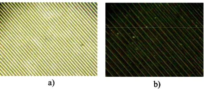
In Fig.4 is shown the electro-optical response of the experimental HAN cell with cell gap of about 4µm. The cell is filled with the liquid crystal material MDA-05-187 (∆ε<0) (Merck). The direction of the
planar orientation is along the comb-like electrode fingers so that Ey component of the fringe field is
a) b)
a) b)b)
Fig. 4. Field-on (a) and field-off (b) states of the experimental cell with the HAN configuration.
directed perpendicular to the HAN deformation plane XZ (see Fig. 2). The observed switching is fast with rise and fall time τr=0.9ms and τf=2ms, respectively,
1-3 / L. Komitov
• IMID 2009 DIGEST
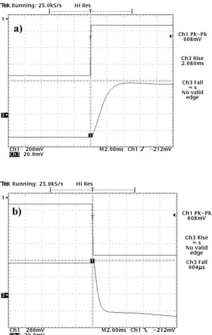
Fig. 5. Electro-optic response of the experimental cell with HAN configuration at applied monopolar voltage of 6V. Notice that the rise τr and fall time τf
indicated on the photographs correspond actually to the measured values of the τf and τr time,
respectively.
3. Summary
The electro-optic response in conventional nematic LCDs arises from the switching of the liquid crystal bulk due to the coupling of the applied electric field with the dielectric anisotropy of the liquid crystal (dielectric coupling). Such kind of switching, however, is slow since it involves the whole bulk of the liquid crystal layer. When instead of dielectric coupling for switching of the liquid crystal is used the flexoelectric one, for instance, than the switching exhibits another features. It is a polar and gives rise to short rise and fall times. If the applied electric field is localized at the substrate surface and the flexoelectric polarization of the liquid crystal is maximum at this surface then the switching of the liquid crystal in the LCD becomes much faster because of two reasons:
a) the bulk molecules are not involved in the
switching process
b) the switching is due to the coupling between the flexoelectric polarization of the nematic liquid crystal and the applied electric field It has been demonstrated in this work fast switching in HAN LCD due to the coupling of the flexoelectric polarization with a fringe field generated by comb-like electrode structure at one of the sample substrates. This coupling seems to be a promising candidate for display applications requiring short switching times and enhanced viewing angle.
Acknowledgement
The author is grateful to Dr.Shinichi Komura (Hitachi Ltd) for the supply of substrates with comb-like electrodes.
5. References
[1] R.B.Meyer, Phys.Rev.Lett., 22, p.918 (1969). [2] S.H.Lee, S.L.Lee, H.Y.Kim, Appl.Phys.Lett.,73,
p.2881 (1998).
[3] Z.Meng, H.Kwok, M.Wong, JSID, 8, p.139 (2000).
a)