44-2 / T. -J. Ha
IMID 2009 DIGEST •
The Effect of Light on Amorphous Silicon Thin Film Transistors based on
Photo-Sensor Applications
Tae-Jun Ha, Hyun-Sang Park, Sun-Jae Kim, Soo-Yeon Lee and Min-Koo Han
School of Electrical Engineering and Computer Science, Seoul National University, Gwanak-gu, Seoul, Korea
[email protected]
ABSTRACT
We have investigated the effect of light on amorphous silicon thin film transistors based photo-sensor applications. We have analyzed the instability caused by electrical gate bias stresses under the light illumination and the effect of photo-induced quasi-annealing on the instability. Threshold voltage (VTH) under the negative gate bias stress with light
illumination was more decreased than that under the negative gate bias stress without light illumination even though VTH
caused by the light-induced stress without negative gate bias was shifted positively. These results are because the increase of carrier density in a channel region caused by the light illumination has the enhanced effect on the instability caused by negative gate bias stress. The prolonged light illumination led to the recovery of shifted VTH caused by negative gate bias
stress under the light illumination due to the recombination of trapped hole charges.
INTRODUCTION
The hydrogenated amorphous silicon thin film transis-tors (a-Si:H TFTs) have attracted considerable attention as uniform and cheap devices for various displays [1-2]. The a-Si:H TFTs have been normally used as switching devices of liquid crystal display. In this application, a-Si:H TFTs have been blocked by using the black matrix which pre-vents the light from being transmitted between the pixels. Hence, the effect of light including the instability caused by light induced stress on a-Si:H TFTs has not be needed to consider. However, a-Si:H TFTs are being applied in pho-to-sensor applications such as touch-screen technology re-cently because a-Si:H TFTs exhibit high photoconductivity. Since a-Si:H TFTs as photo sensors have to be exposed to light illumination directly, the effect of light on a-Si:H TFTs has become an issue.
It has been reported that a-Si:H TFTs have the unstable characteristics such as threshold voltage (VTH) shift and sub-threshold slope (S.S.) change when prolonged electric-al bias stress to the gate electrode was applied [3-6]. The mechanisms to explain the instability caused by electrical gate bias stresses on a-Si:H TFTs have so far been studied
[3-6].
In particular, the unexpected instability of a-Si:H TFTs due to the effect of light under electrical gate bias can lead failure in the operation for demanding photo-sensor appli-cations. Nonetheless, the mechanism to explain instability caused by light-induced stress under electrical gate bias has not been investigated enough to be applied to photo-sensor applications. Recently, we have researched the ways to recover the instability caused by negative gate bias stress using the light-induced condition.
The purpose of our work is to investigate the effect of light on amorphous silicon thin film transistors based on light-sensor applications. We have analyzed the instability caused by electrical gate bias stresses under the light illu-mination and the effect of photo-induced quasi-annealing on the instability.
EXPERIMENT
We fabricated the inverted-staggered bottom gate a-Si:H TFTs by using etch-back process. First, a 250 nm thick double-layer gate metal (Mo/AlNd) was deposited by DC sputtering on a glass substrate. 450nm thick SiNx gate insulator layer, 200 nm thick a-Si:H active layer and 50 nm thick N+ doped a-Si:H layer were deposited by plas-ma-enhanced chemical vapor deposition (PECVD) in turn. After active island patterned, a 450 nm thick triple-layer source and drain electrode (Mo/AlNd/Mo) was deposited by sputtering. The 105 nm N+ doped a-Si:H layer between the source and drain electrode was dry etched to form the etch-back-type channel after patterning the source and drain electrode by a wet etching. A 200 nm thick SiNx was deposited for a passivation. Finally, after contact holes were formed, an indium tin oxide (ITO) electrode was de-posited and patterned. The dimension of a-Si:H is 200 µm¯5 µm.
The experiment temperature was 333 K. The source of light had luminance of 20,000 lx. The voltage between the drain and source electrode was fixed as 0V. The stress time was 20,000 seconds. The a-Si:H TFTs samples were
an-44-2 / T. –J. Ha
• IMID 2009 DIGEST
nealed at 200℃ for 30 minutes before experiments. The measurements were performed under both dark (0 lx) state and illuminated (20,000 lx) state.
RESULTS AND DISCUSSION
After the light-induced stress without electrical gate bi-as wbi-as applied to a-Si:H TFT, figure 1 shows that VTH was increased from 1.08 V to 3.42 V. In addition, S.S. was in-creased from 0.80 V/dec to 1.31 V/dec. VTH shift and S.S. change caused by light-induced stress on a-Si:H TFTs could be a result of Staebler-Wronski effect (SWE) [7-8]. The SWE effect is caused by the defect creation of dan-gling-bond broken near mid-gap at the interface between a-Si:H layer and gate insulator. Generated defect states slow down the movement of the Fermi level toward the conduction band. It was shown as VTH increase and S.S. increase of I-V transfer curve. In addition, the characteristic of self-recovery after light-induced stress was investigated. As shown in figure 1, I-V transfer curve after keeping floating-state (no contact, no heat) for 20000 seconds was hardly changed. It supports that generated defect states are hard to be self-recovered without thermal annealing as re-ported [4-5]. -15 -10 -5 0 5 10 15 10-14 10-13 10-12 10-11 10-10 10-9 10-8 10-7 10-6 10-5 VDS = 0.1 V D rai n C u rr ent (A ) Gate-Source Voltage (V) initial stress 20000sec floating 20000sec
light stress without negative gate bias W/L = 200/5
T= 333K
Figure.1 I-V transfer curve after light-induced stress without electrical gate bias
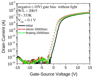
As shown in figure 2, VTH was decreased from 1.28 V to -1.14 V after a-Si:H TFT was subject to -10V gate bias stress. However, S.S. was hardly changed. This result means that holes are trapped into gate insulator by negative gate bias stress [9]. This is because why the trapped holes
are formed as charge sheet so that those function as positive offset for the gate voltage. In the case of negative gate bias stress, the characteristic of self-recovery was experimented. As shown in figure 2, I-V transfer curve after keeping floating-state for 20000 seconds was recovered but not much. The results support that shallow-trapped charges at the interface between a-Si:H active layer and gate insulator may be released as time goes by. Therefore, the instability caused by negative gate bias stress has the different mechanism from that caused by light-induced stress.
-15 -10 -5 0 5 10 15 10-14 10-13 10-12 10-11 10-10 10-9 10-8 10-7 10-6 10-5 VDS = 0.1 V D
rain Current (A)
Gate-Source Voltage (V)
initial
stress 20000sec floating 20000sec
negative (-10V) gate bias without light W/L = 200/5
T= 333K
Figure 2 the I-V transfer curve of a-Si:H TFTs after negative gate bias stress without the light illumination
To support the mechanism of instability caused by negative gate bias stress, the negative gate bias stress was applied for 20000 seconds after only light-induced stress for 20000 seconds. Figure 3 shows that positively shifted VTH caused by light-induced stress was negatively shifted without changing S.S. after negative gate bias stress without light illumination. This result means that the instability caused by negative gate bias stress is due to the trapped hole charges into gate insulator regardless of generated defect states caused by light-induced stress [9]. The trapped holes are formed as charge sheet so that those function as positive offset for the gate voltage. Therefore, negative VTH shift in I-V transfer curve of a-Si:H TFT was observed while maintaining S.S. In addition, since trapped holes may be released as time goes by, self-recovery could happen as shown in figure 2. However, it is very difficult for deep-trapped charges to be fully recovered without thermal annealing.
44-2 / T. -J. Ha IMID 2009 DIGEST • -25-20-15-10 -5 0 5 10 15 20 25 10-13 10-12 10-11 10-10 10-9 10-8 10-7 10-6 10-5 10-4 VDS = 0.1 V Drai n Curr ent ( A ) Gate-Source Voltage (V) initial
light-induced stress for 20000s - (1) negative gate stress after (1)
Negative gate stress after light-induced stress W/L = 200/5
T =333K
Figure 3 I-V transfer curve after negative gate stress on light-induced stressed a-Si:H TFT
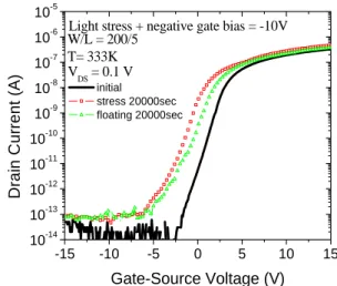
To examine the effect of the light illumination under negative gate bias on the instability of a-Si:H TFTs, light-induced stress under negative (-10 V) gate bias was applied. Figure 4 shows that VTH was decreased from 1.31 V to -3.70 V. The VTH after negative gate bias stress with light illumination was more decreased than that after nega-tive gate bias stress without light illumination. In other words, the instability caused by negative gate bias stress was enhanced due to the effect of light in spite of the dif-ferent mechanism of the instability caused by the light-induced stress. It can be expected that the effect of light is related with the mechanism of instability caused by negative gate bias stress. In the case of negative gate bias stress under the light illumination, I-V transfer curve was more recovered as shown in figure 4 when compared with that in figure 2. It is induced that at first more hole charges were trapped at the interface during the stress due to the effect of light and naturally released during the floating time.
Light illumination increased carrier density when the light-induced stress was applied to a-Si:H TFTs [10-11]. At the same time extended hole-accumulation channel was formed by applied negative gate bias. Hence, the mechan-ism of charge trapping was promoted due to the increase of hole density in a channel region. This is because the in-creased holes in a channel region appertain to the source of the mechanism. It is concluded that larger VTH shift caused by light-induced stress under negative gate bias results from the increase of hole density in a channel region by light illumination. The increase of carrier density in a channel region caused by the light illumination has the
en-hanced effect on the instability caused by negative gate bias stress. -15 -10 -5 0 5 10 15 10-14 10-13 10-12 10-11 10-10 10-9 10-8 10-7 10-6 10-5 VDS = 0.1 V D rai n C u rrent (A) Gate-Source Voltage (V) initial stress 20000sec floating 20000sec
Light stress + negative gate bias = -10V W/L = 200/5
T= 333K
Figure 4 I-V transfer curve after negative (-10 V) gate bias stress with and without light illumination
As shown in figure 5, the prolonged light illumination led to the recovery of shifted VTH caused by negative gate bias stress under the light illumination as thermal post-annealing treatment on stressed TFTs. The results in figure 5 were contrasted with those in figure 1, 2 and 4 which represent little self-recovery under the floating state. In other words, the effect of light on stressed a-Si:H TFT was observed as the recovery to initial state. This is be-cause the recombination of even deep-trapped hole charges can be generated by the light illumination.
However, as shown in figure 5, increased S.S. caused by the light-induced stress was not improved even though shifted VTH was recovered. It also supports that the effect of photo-induced quasi-annealing is connected with trapped hole charges caused by negative gate bias not generated defect states caused by light-induced stress. Hence, the in-stability caused by negative gate bias stress under the light illumination can be suppressed by using the effect of pho-to-induced quasi-annealing with time-division method on a-Si:H TFT based on photo-sensor applications as well as AMOLED displays.
44-2 / T. –J. Ha • IMID 2009 DIGEST -15 -10 -5 0 5 10 15 10-14 10-13 10-12 10-11 10-10 10-9 10-8 10-7 10-6 10-5 VDS = 0.1 V Dr a in Cu rr e n t (A ) Gate-Source Voltage (V) initial
light+neg stress 20000sec only light stress 20000sec
W/L = 200/5 T= 333K a) -20 -15 -10 -5 0 5 10 15 20 25 10-12 10-11 10-10 10-9 10-8 10-7 10-6 10-5 10-4 VDS = 0.1 V D rai n C u rr ent ( A ) Gate-Source Voltage (V) initial
light+negative (-10V) stress 20000sec only light stress 20000sec
Under illuminated condition W/L = 200/5
T= 333K
b)
Figure 5 the recovery of the instability after photo-induced quasi-annealing measured a) under the dark condition b)
under the illuminated condition
CONCLUSION
We have investigated the effect of light on amorphous sil-icon thin film transistors based photo-sensor applications. We have analyzed the instability caused by electrical gate bias stresses under the light illumination and the effect of pho-to-induced quasi-annealing on the instability. VTH under the
negative gate bias stress with light illumination was more de-creased than that under the negative gate bias stress without
light illumination even though VTH caused by the light-induced
stress without negative gate bias was shifted positively. These results are because the increase of carrier density in a channel region caused by the light illumination has the enhanced effect on the instability caused by negative gate bias stress. The pro-longed light illumination led to the recovery of shifted VTH
caused by negative gate bias stress under the light illumination due to the recombination of trapped hole charges.
The investigation of the effect of light on a-Si:H TFTs can present physical characteristics of devices and limita-tion of operalimita-tion when applied to the circuit design of pho-to-sensor applications. In particular, the instability caused by electrical gate bias under the light illumination can be overcome throughout the effect of photo-induced qua-si-annealing.
REFERENCES
[1] T.Shirasaki et al., Proc. International display workshop, 275-278 (2004)
[2] Jiin-Jou Lih et al., SID International Symposium Pro-ceedings, 1504 (2004)
[3] M. J. Powell et al., Appl. Phys. Lett., vol. 43(6), 15 pp. 597-599 (1983).
[4] C.van Berkel et al., Appl. Phys. Lett., Vol.51, p.1094 (1987)
[5] M. J. Powell et al., Appl. Phys. Lett., vol. 51(16), 19 pp. 1242-1244 (1987).
[6] C.F.O.Graeff et al., Physical Review B., vol.52 7. pp. 4680-4683 (1995) .
[7] Lihong(Heidi) Jiao et al., Material Research Society, vol. 910 (2006).
[8] Norio Inui et al., J.J.Appl. Phys, vol. 45, 3A pp. 1675-1679 (2006).
[9] M. J. Powell et al., Physical Review B., vol. 45, 8 pp. 4160-4170 (1991).
[10] M. Stutzmann et al., Physical Review B, pp. 23-47 (1985).
[11] Lihong(Heidi) Jiao et al., Material Research Society, vol. 910 (2006).