50-3 / J. K. Jeong
IMID 2009 DIGEST •
Abstract
The two approaches to improve the stability of oxide TFTs are described. First approach is the optimization of device architecture including MIS structure and passivation layer using conventional InGaZnO semiconductor channel layer. Second approach is to develop the new kinds of oxide semiconductor materials, which is very robust and stable against the gate bias stress and thermal stress.
1. Introduction
Recently, ZnO-based transistors have been intensively investigated for the active-matrix backplane of AMOLED display.[1-4] Although the high performance ZnO-based TFTs have been successfully fabricated, there is the most critical stability issue to be resolved. In this paper, the degradation mechanisms of the threshold voltage were discussed for the bottom–gate InGaZnO TFTs. The improvement in the DC stability of InGaZnO TFT was demonstrated by optimizing the passivation layer, based on the proposed mechanism framework. As a second approach, the new ZrInZnO semiconductor was investigated. Some preliminary experimental data were presented.
2. Experimental
Lithographically patterned Mo (200nm) on a
SiO2/glass substrate with a surface area of
370×400mm2 was used as the gate electrode. SiN x
(120nm) film as a gate dielectric layer was deposited by PECVD at a substrate temperature of 390°C. The
a-IGZO film with a thickness of 50nm was grown by
dc sputtering on a SiO2/glass substrate with a surface
area of 370×400mm2 using a polycrystalline
In2Ga2ZnO7 target at room temperature. The
sputtering was carried out at a gas mixing ratio of Ar/O2 = 72/28 and an input power of 1200W. After
defining the a-IGZO channel using photolithography
and wet etching, a SiOx passivation layer was
deposited by PECVD and then patterned by dry etching. A device with a PA layer as a passivation layer was also fabricated: the PA layer was formed using a photo-resist coater and developed to define the source/drain contact region. Mo source and drain electrodes (200nm) were formed by sputtering and then patterned by photolithography and subsequent dry etching. Finally, the sample was subjected to thermal annealing at 250oC for 1hr.
3. Results and discussion
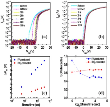
Most of the degradation mechanisms regarding ZnO-based TFT were ZnO-based on the stretched exponential model, which has been useful for interpretation of amorphous Si TFTs. However, the Vth instability in
oxide TFT is quite difference because the ZnO-based materials are extremely sensitive to the partial pressure of oxygen and water molecules. Figure 1(a) and (b) show the evolution of the transfer curves as a function of the applied stress time for the organic passivated device (device A) and inorganic passivated device (device B), respectively. The devices were stressed under following conditions: the IDS was set to
10µA and the VDS was fixed at 5.1V. The maximum
stress duration was 36,000sec. Although the Vth for
the device A was strongly shifted by approximately 8.1V from 5.5 to 13.6V, the positive Vth shift in device
The strategy for the fabrication of oxide TFTs with excellent device stabilities: The novel oxide TFT
Jae Kyeong Jeong,
1* Jin-Seong Park,
2Yeon-Gon Mo,
2and Hye Dong Kim
21
Dept. of Materials Science and Engineering, Inha University,
Incheon 402-751, South Korea
Tel.:82-32-860-7524, E-mail: [email protected]
2
Technology Center, Samsung Mobile Display, Yongin-si,
Kyunggi-do 449-902, South Korea
50-3 / J. K. Jeong
• IMID 2009 DIGEST
B was very small (~2.0V) after a constant drain current stress of 36,000sec.
Fig. 1. The evolution of the transfer curves for the (a) PA-passivated and (b) SiOx-passivated IGZO
transistors as a function of the applied stress time (W/L = 25/10 µm). The variations in the (c) Vth
shift and (d) S value for the PA-passivated and SiOx-passivated IGZO transistor as a function of
stress time.
The positive Vth shift of oxide TFTs under positive
gate voltage stress has been explained by two models: charge trapping or defect creation.[5-8] While the parallel shift in Vth without significant change in the
SS value during stress time is attributed to simple charge trapping in the gate dielectric and/or at the channel/dielectric interface, the positive shift of Vth
accompanying the change in S comes from the creation of defects within the oxide semiconductor channel material. In this study, because devices A and B have an identical gate dielectric and IGZO semiconductor, the charge trapping at or near the channel/dielectric interface during gate voltage stress would be expected to be similar to each other. However, the positive Vth shifts for devices A and B
were 8.1V and 2.0V, respectively. Therefore, the charge trapping model alone cannot entirely account for the results obtained. We believed that the gate bias induced-Vth instability comes from the interaction
between the IGZO back-surface and ambient (O2,
H2O). Indeed, it was found that the positive Vth shift
under the positive gate voltage stress is greatly dependent on the presence and film quality of the passivation layer.
Fig. 2. Dependence of the Vth shift on the gate bias
stresses for both devices A and B. For comparison, the effect of the gate bias stress on the unpassivated oxide transistor was also included.
Figure 2 shows the effect of the passivation layer on the Vth instability of IGZO TFT under the constant
gate voltage stress. The oxide TFT with the passivation layer of the dense SiO2 exhibited the
excellent DC stability, compared to that of the unpassivated TFTs. This result can be explained by
the following consideration: in the dense SiO2
passivated device, the adsorption of additional oxygen from the ambient atmosphere is kinetically prevented by the diffusion barrier property of the SiOx thin film
(100nm), thereby resulting in a much smaller Vth shift
(0.42V).[9]
From this experimental result, it is evident that the immune active channel layer against the ambient atmosphere and bias stress is crucial for the excellent Vth stability. Thus, the new ZrInZnO thin film was
synthesized by cosputtering of InZnO target and ZrO2
target.[10]
Figures 3(a) and (b) show selective area diffraction patterns (SADP) of the as-deposited and annealed samples, respectively. It can be shown that the inter-planar spacing of as-deposited film (a, b, and c in Fig. 3(a)) is larger than that of annealed film by approximately 0.1~0.2 Å. This result is consistent with that obtained from the XRD analysis discussed earlier. In addition, the serial diffraction ring patterns can be interpreted by the body-centered-cubic (BCC) system (In2O3 based structure) rather than a simple
50-3 / J. K. Jeong
IMID 2009 DIGEST • (d) show a bright-field image and a high-resolution
electron microscopy image of an as-deposited sample, respectively. These indicate that nano-crystals with sizes between 20-30nm are non-uniformly distributed and embedded in an amorphous matrix. In addition, the nanoscale crystallites have spherical shapes in the as-deposited ZrInZnO film and they are surrounded by amorphous layers of thickness in the range 3-4nm. To confirm the composition of the crystal phases, the scanning transmission electron microscopy high angle annular dark-field (STEM-HAADF) method and energy dispersion X-ray spectroscopy (EDS) have been used on the as-deposited samples. As shown in Figure 3(e), there are zirconium, indium, zinc, and oxygen elements in each crystal which suggests that the nano-crystals are composed of the solid solution phase of the ZrInZnO compound. On the other hand, the bright-field image of the annealed sample (350°C)
is shown in Figure 3(f) where the distribution of the nano-crystals in the annealed film tends to be more uniform and the thickness of the amorphous phase between the crystallites is seen to be significantly reduced from 3~4nm to 1nm. This indicates that the grain growth of nano-crystallites sacrificing the amorphous matrix occurs during the high temperature annealing due to Ostwald ripening.
Fig. 3. TEM analysis of ZrInZnO film (Zr:In:Zn = 0.19:0.61:0.20). SADP of (a) as-deposited film and (b) film annealed at 350°C, based on bcc In2O3
structure. (c) Bright-field and (d) high-resolution
TEM images of as-deposited ZrInZnO films. (e) STEM-HAADF and EDS spectrum of the as-deposited ZrInZnO films. (f) Bright-field image of ZrInZnO film annealed at 350°C.
The representative output characteristics of Zr0.4In1.2Zn0.4O3 TFTs annealed at 350°C for 2hrs are
shown in Figure 4(a). At low VDS, the IDS increased
with increasing VGS due to the enhanced accumulated
charge density at the ZrInZnO/SiNx interface. In
addition, a clear pinch-off and drain current saturation indicates that the electron transportation in active channels is totally controlled by the gate and drain voltages. Figure 4(b) shows the transfer characteristics of the Zr0.4In1.2Zn0.4O3 TFTs annealed at 350°C for
2hrs. ZrInZnO TFTs with n-channel conduction exhibited a field-effect mobility of 3.9cm2/Vs, an S
value of 0.98V/decade, a Vth of 1.6V and an Ion/off ratio
of approximately 107. These values are comparable to
those observed in typical ZnO-based TFTs.
Fig. 4. The (a) output and (b) transfer characteristics of ZrInZnO TFTs annealed at 350°C. The transfer curve after 60hr bias stress is
also shown in Figure 4(b).
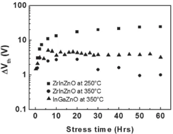
The important stability issue of TFTs with a ZrInZnO channel layer has been investigated and compared with that of InGaZnO TFTs. A drain current stress of 3µA at VDS=10V was applied into the sample
50-3 / J. K. Jeong
• IMID 2009 DIGEST
for a period of 60 hrs. The variation of Vth for the
ZrInZnO TFT device during the application of the on-state current stress is shown in Figure 5. The stabilities of the InGaZnO TFTs sample annealed at 350°C as well as the ZrInZnO TFTs one annealed at
250°C and 350°C have been compared. The 250°
C-annealed ZrInZnO device showed a large positive shift (~24V) in Vth after the application of the bias
stress for 60 hrs. However, the 350°C-annealed
ZrInZnO device exhibited a dramatic improvement; namely that only a 0.99 V shift in Vth was observed
after the same stress application and these overall transfer characteristics was shown in the inset of Figure 4(b). It is noted that the Vth shift of
co-sputtered IGZO TFT devices under identically
stressed conditions (IDS=3µA, t=60hrs) have been
found to be approximately 3.4V, as shown in Figure 5. Therefore, it is conclude that Zr doping of the InZnO material would be a useful route for producing more reliable TFTs, which are needed for realizing acceptable driving transistors for AMOLED displays.[10]
Fig. 5. The variation of Vth for ZrInZnO TFTs
annealed at 250 and 350°C as a function of time of
applied bias stress. The stability data for a InGaZnO TFT annealed at 350°C is also presented.
4. Summary
The origin of Vth instability in InGaZnO TFT was
studied based on the concept of the electrically-induced chemical reaction between the bare InGaZnO surface and ambient atmosphere (O2, H2O) for the first
time. This viewpoint was verified by the stability
comparisons for the unpassivated and SiO2-passivated
InGaZnO TFTs. In addition, the newly designed ZrInZnO material exhibited the excellent DC stabilities as well as the interesting crystallographic properties.
5. References
[1] K. Nomura, H. Ohta, A. Takagi, T. Kamiya, M.
Hirano, and H. Hosono, Nature (London) 432,
488 (2004).
[2] E. Fortunato, P. Barquinha, A. Pimentel, A.
Goncalves, A. Marques, L. Pereira, and R. Martins, Adv. Mater. (Weinheim, Ger.) 17, 590 (2005).
[3] J. K. Jeong, J. H. Jeong, H. W. Yang, J.-S. Park,
Y.-G. Mo and H. D. Kim, Appl. Phys. Lett. 91, 113505 (2007).
[4] M. Kim, J. H. Jeong, H. J. Lee, T. K. Ahn, H. S.
Shin, J.-S. Park, J. K. Jeong, Y.-G. Mo and H. D. Kim, Appl. Phys. Lett. 90, 212114 (2007).
[5] R. B. M. Cross and M. M. De. Souza, Appl. Phys.
Lett. 89, 263513 (2006).
[6] P. Gorrn, P. Holzer, T. Riedl, W. Kowalsky, J.
Wang, T. Weimann, P. Hinze and S. Kipp, Appl. Phys. Lett. 90, 063502 (2007).
[7] Y. Vygranenko, K. Wang and A. Nathan, Appl.
Phys. Lett. 91, 263508 (2007).
[8] A. Suresh and J. F. Muth, Appl. Phys. Lett. 92,
033502 (2008).
[9] J. K. Jeong, H. W. Yang, J. H. Jeong, Y.-G. Mo
and H. D. Kim, Appl. Phys. Lett. 93, 123508,
(2008).
[10] J.-S. Park, K. S. Kim, Y.-G. Park, Y.-G. Mo, H.
D. Kim, and J. K. Jeong, Advanced Materials. 21, 329 (2009).