Surface property controllable multilayered gate dielectric for low voltage organic
thin film transistors
Sung Jin Jo, Chang Su Kim, Jong Bok Kim, Joohee Kim, Min Jung Lee, Hyeon Seok Hwang, Hong Koo Baik, , and Youn Sang Kim,
Citation: Appl. Phys. Lett. 93, 083504 (2008); doi: 10.1063/1.2973160 View online: http://dx.doi.org/10.1063/1.2973160
View Table of Contents: http://aip.scitation.org/toc/apl/93/8 Published by the American Institute of Physics
Surface property controllable multilayered gate dielectric for low voltage
organic thin film transistors
Sung Jin Jo,1Chang Su Kim,1Jong Bok Kim,1Joohee Kim,2Min Jung Lee,2 Hyeon Seok Hwang,1Hong Koo Baik,1,a兲 and Youn Sang Kim2,b兲
1
Department of Materials Science and Engineering, Yonsei University, Seoul 120-749, South Korea
2
Center for Intelligent Nano-Bio Materials, Department of Chemistry and Nano Science (BK 21), Ewha Womans University, Seoul 120-750, South Korea
共Received 9 June 2008; accepted 13 July 2008; published online 26 August 2008兲
We report the effects of dielectric surface properties on the device performance of organic thin film transistors 共OTFTs兲 using polymer/high-k oxide multilayered gate dielectrics. We systematically controlled the surface energy of the gate dielectric from very hydrophobic to very hydrophilic. The modified dielectric surface strongly affected the initial growth mechanism of pentacene and subsequently the performance of the OTFTs. The performance of the OTFTs with a higher surface energy was superior to that of the OTFTs with a lower surface energy. © 2008 American Institute of Physics.关DOI:10.1063/1.2973160兴
Organic thin film transistors共OTFTs兲 have been studied extensively over the past few decades and are expected to lead the future of organic electronics.1 However, the high operating voltage共over 50 V兲, which is attributed to the low dielectric constant of the common organic dielectric layer, remains a limitation of OTFTs. Recently, we introduced polymer/high-k oxide double gate dielectrics to increase the gate capacitance as well as to retain the advantages from the both organic and inorganic dielectrics.2,3The dielectric sur-face chemical modification can dictate the electrical perfor-mance of OTFTs by influencing the morphology and struc-ture of the active layer. It is therefore important to establish precise interfacial control between organic semiconductors/ polymer gate dielectrics in order to achieve higher perfor-mance in low operating voltage OTFTs with a multilayered gate dielectric. However, only a few systematic studies have been carried out to reveal the effects of dielectric surface properties on the device performance of OTFTs using polymer/high-k oxide multilayered gate dielectrics.
In this study, poly共dimethyl siloxane兲 共PDMS兲/high-k yttrium oxide 共YOx兲 was chosen as a multilayered gate
di-electric layer. Since the amount of methyl group on the sur-face of a PDMS dielectric can be controlled by ultraviolet/ ozone 共UVO兲 treatment, we were able to systematically control the surface energy of the gate dielectric from very hydrophobic to very hydrophilic 共contact angle of water is 5 ° – 103°兲. Moreover, this method enabled us to avoid the problems associated with the use of different functional groups, which may provide completely different environ-ments for the organic semiconductor growth.
For the fabrication of the OTFT, heavily doped p-Si wa-fers were used as the substrate and gate electrode. As the inorganic high-k dielectric, YOx films were deposited by
electron beam evaporation at room temperature. Sylgard 184 PDMS prepolymer was mixed thoroughly with its cross-linking catalyst 共10:1 w/w兲 and diluted in trichloroethylene. The diluted PDMS was spin-cast onto a substrate. The UVO
a兲Electronic mail: [email protected]. b兲Electronic mail: [email protected].
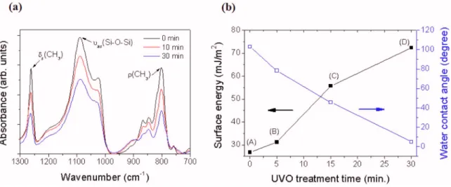
FIG. 1. 共Color online兲 共a兲 FTIR transmission spectra of the PDMS layer at various UVO treatment times. 共b兲 Surface energy and contact angle of water as a function of UVO treatment time for the PDMS layer. Gate dielectrics A, B, C, and D after UVO treatment times of 0, 5, 15, and 30 min, respectively.
APPLIED PHYSICS LETTERS 93, 083504共2008兲
treatment of the PDMS surface was carried out in a commer-cial UVO surface treatment system 共Minuta Tech, Ozone cure 16兲. Pentacene channels were deposited by heating the effusion cell. Finally, the gold was thermally evaporated to form the source/drain electrodes with a channel length of 100 m and width of 2000 m. The electrical characteris-tics of the OTFTs were measured using an Agilent 5270 B semiconductor parameter analyzer.
As shown in Fig.1共a兲, Fourier transform infrared共FTIR兲 measurements were carried out on the PDMS layer in order to delineate the chemical state change of the PDMS layer by UVO treatment. Among the most intense were those associ-ated with CH3 rocking共785–815 cm−1兲, symmetricCH3
de-formations 共1245–1270 cm−1兲, and asymmetric Si–O–Si stretches 共1055–1090 cm−1兲. UVO treatment caused a no-ticeable decrease in the magnitude of different CH3 peaks,
suggesting a gradual disappearance of methyl groups from oxidized molecules of PDMS.4To support the FTIR results, the surface energies of the PDMS layer at various UVO treatment times were measured using the sessile contact angle method. As shown in Fig.1共b兲, an increase in the total surface energy in the PDMS layer was observed with an increased UVO treatment time. Gate dielectrics A, B, C, and
D represent the PDMS layer after UVO treatments of 0, 5, 15, and 30 min, respectively. The FTIR and surface energy measurement results confirmed that the decrease in the num-ber of methyl groups directly is related to the increase in the surface energy of the PDMS layer.
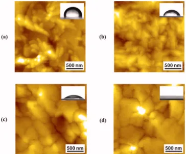
We expected that the difference in surface wetting prop-erties caused by the methyl group density would strongly influence the pentacene growth morphology. Generally, in order to form large pentacene islands in the initial stages of growth, the gate dielectric is required to have a relatively high surface energy that can induce the increased wetting and two-dimensional growth of the pentacene film. More-over, many reports have experimentally demonstrated that pentacene films grown on a hydrophilic surface form large grains.5–7 Shin et al.8 presented that the increased surface energy of a dielectric that results from the oxygen plasma ensures a good wetting of the pentacene on the dielectric surface and enlarges the grain size. As shown in Fig. 2, the pentacene films on dielectrics C and D, having higher sur-face energies, exhibited well-formed dendritic structures and grain sizes around 1 – 2 m. However, on gate dielectric B, having a lower surface energy, the pentacene film did not show any dendritic structure and its grain size was reduced to less than 0.2 m. Also, the pentacene film on dielectric A showed very rough surface morphology with inclined grains and many voids; this presumably occurred because the inter-action between the pentacene and the CH3-functional group
was too severe.9
To correlate the pentacene morphology described above with the electrical properties of the OTFTs, transistors were fabricated. As shown in Fig.3, all the TFT performance char-acteristics, particularly carrier mobility, were considerably improved as the UVO treatment time increased. The carrier mobilities of the TFTs with gate dielectrics A, B, C, and D were 0.002, 0.259, 0.897, and 2.124 cm2/V s, respectively. As discussed above, the enhancement of carrier mobility may be attributed to the growth mode change of pentacene. A decrease in the grain size of the organic semiconductor reduces the carrier mobility of the OTFTs. It is clearly seen from Fig. 2 that the pentacene grain size increased as the UVO treatment time increased. Moreover, it is known that in the OTFTs, the carriers induced by the gate bias are located within a few monolayers just above the dielectric layers. Thus, to understand the origin of the mobility enhancement more precisely, the morphology of the pentacene film was investigated in detail during the initial growth step. Figure4 FIG. 2. 共Color online兲 Tapping mode AFM topographic images of 50 nm
thick pentacene films deposited on a PDMS/YOxlayer at various UVO
treatment times:共a兲 UVO 0 min, 共b兲 UVO 5 min, 共c兲 UVO 15 min, and 共d兲 UVO 30 min. Inset shows water droplet images on a PDMS/YOxlayer.
FIG. 3. 共Color online兲 Transfer characteristics of pentacene TFTs fabricated on a PDMS/YOxlayer at various UVO treatment times:共a兲冑ID-VGand共b兲
log共ID兲-VG curves.
shows AFM images of the pentacene films grown on dielec-trics B and C with nominal thickness increasing from 1 to 10 nm. The morphology of pentacene on gate dielectric B was strikingly different from that on gate dielectric C. On gate dielectric B, the process of island coalescence was more lim-ited, whereas the adjacent islands coalesced to form larger islands in the case of gate dielectric C. The vacant space between islands did not decrease appreciably for the penta-cene films on gate dielectric B, and large vacant spaces be-tween grains were observed even at a film thickness of 5 nm. These results strongly suggest that different pentacene growth mechanisms are involved according to the surface state of the gate dielectric layer.
To provide a quantitative basis for the growth mode change of pentacene film on gate dielectrics B and C, we have calculated the work of adhesion between pentacene and the gate dielectric. Since the work of adhesion共Wa兲 between
materials can be defined by the relationship involving sur-face energies and interfacial energy as follows, the Volmen– Weber mode is favored when Wa⬍2␥f and the Frank–van
der Merwe mode is favored when Wa⬎2␥f.10
Wa=␥f+␥s−␥i= 4␥f d␥ s d ␥f d +␥s d− 4␥f p␥ s p ␥f p +␥s p, 共1兲
where d and p represent the dispersion and polar components of the surface tension, respectively. The calculated works of adhesion from Eq. 共1兲 are Wa= 66.0 mJ/m2 for pentacene
and gate dielectric B and Wa= 83.2 mJ/m2for pentacene and
gate dielectric C. The surface energy of pentacene was also measured by the contact angle method and the value was 35.1 mJ/m2. Thus, the Volmen–Weber mode was observed
on gate dielectric B, while the Frank–van der Merwe mode was observed on gate dielectric C. Considering that charge transport occurs dominantly at a few pentacene monolayers, Frank–van der Merwe growth is desired for transistor appli-cations because it leads to large, well-connected domains that facilitate a charge transport parallel to the substrate. In-deed, at a nominal thickness of 5 nm, the ratio of the grain
area on dielectric B was increased from 68.7% to 88.7% on dielectric C. This indicated that the voids between the islands that disturb the carrier transport were reduced when the pen-tacene film was deposited on gate dielectric C.
In summary, we investigated the semiconductor/ dielectric interface chemical effects on low voltage OTFT performance. The present results for OTFTs fabricated on multilayered gate dielectrics having a wide range of surface chemical states provide new insights into the critical rela-tionships between OTFT performance parameters and semi-conductor growth mechanisms.
This work was supported by the SRC Program of MOST/KOSEF through the Center for Intelligent Nano-Bio Materials at Ewha Womans University共Grant No. R11-2005-008-00000-0兲, the Seoul Research and Business Develop-ment Program 共Grant No. 10816兲, and the “SystemIC2010” Project of Korea Ministry of Knowledge Economy. Also, the authors are appreciative of the financial support from LG Display.
1M. Cavallini, P. Stoliar, J. Moulin, M. Surin, P. Leclere, R. Lazzaroni, D.
W. Breiby, J. W. Andreasen, M. M. Nielsen, P. Sonar, A. C. Grimsdale, K. Mullen, and F. Biscarini,Nano Lett. 5, 2422共2005兲.
2C. S. Kim, S. J. Jo, S. W. Lee, W. J. Kim, H. K. Baik, and S. J. Lee,Adv.
Funct. Mater. 17, 958共2007兲.
3S. J. Jo, C. S. Kim, M. J. Lee, J. B. Kim, S. Y. Ryu, J. H. Noh, K. Ihm, H.
K. Baik, and Y. S. Kim,Adv. Mater.共Weinheim, Ger.兲 20, 1146共2008兲. 4K. Efimenko, W. E. Wallace, and J. Genzer,J. Colloid Interface Sci. 254,
306共2002兲.
5S. Kang, S. Jung, J. Park, H. Lee, and M. Yi,Microelectron. Eng. 84,
1503共2007兲.
6D. Guo, S. Entani, S. Ikeda, and K. Saiki,Chem. Phys. Lett. 429, 124
共2006兲.
7M. W. Lee and C. K. Song,Jpn. J. Appl. Phys., Part 1 42, 4218共2003兲. 8K. Shin, S. Y. Yang, C. Yang, H. Jeon, and C. E. Park,Appl. Phys. Lett.
91, 023508共2007兲.
9M. Halik, H. Klauk, U. Zschieschang, G. Schimid, C. Dehm, M. Schutz,
S. Maisch, F. Effenberger, M. Brunnbauer, and F. Stellacci, Nature 共London兲 431, 963共2004兲.
10S. Wu,J. Adhes. 5, 39共1973兲.
FIG. 4. 共Color online兲 2⫻2 m2AFM images of pentacene films deposited on a PDMS/YO
xlayer with nominal thicknesses of 1, 3, 5, and 10 nm,
respectively. UVO treatments for共a兲 5 min and 共b兲 15 min.