P1-94 / E. Y. Nam
IMID 2009 DIGEST •
Abstract
In this work, pyromellitic dianhydride (PMDA) was used as a cathode interfacial layer in the organic light emitting diodes (OLEDs) and its thickness was optimized. Various electrical and optical characterizations of the OLEDs having various thicknesses of the PMDA cathode interfacial layer revealed that the best OLED performance could be achieved by using 0.5 nm-thick PMDA layer compared to the control device without any interfacial layer.
1. Introduction
The organic light emitting diode (OLED) is one of the most promising display devices in the future flat panel application.1 Its major advantages can be
emphasized to be low-power consumption, excellent emission quality with a wide-view angle, and color tuning capability. However, its electroluminescent efficiency still needs further improvement and balancing the numbers of electrons and holes injected into the organic light emitting layer is the most important parameter to be engineered. Up to now, the most significant improvement of the OLED performance was achieved by using an ultra-thin LiF as an interfacial layer between the cathode and the organic layer.2
In this presentation, as an alternative cathode interfacial layer, we used pyromellitic dianhydride (PMDA) film with various thicknesses (0.3 – 1.3 nm) between the tirs-(8-hydroxyquinoline) aluminum (Alq3) and Al cathode, and tried to find the most
optimum thickness showing the best OLED performance.
2. Experimental
The OLED devices with various PMDA thicknesses as a cathode interfacial layer were fabricated on the ITO- coated glass. After cleaning the substrates, N,N′- diphenyl-N,N′-bis(3-methylphenyl)-1,1′-diphenyl-4,4′-diamine (TPD) and tris-(8-hydroxyquinoli ne) aluminum (Alq3) were deposited as a hole transport
layer (HTL) and an emitting material layer (EML), respectively. In order to find the optimum OLED configuration, the PMDA cathode interfacial layers having a thickness ranged from 0.3 to 1.3 nm were deposited and the Al was used as a cathode electrode. All the layers used in our OLED fabrication were deposited by using a thermal evaporation method.
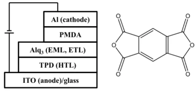
Fig.1 shows the schematic cross-sectional device configuration and the molecular structure of PMDA.
ITO (anode)/glass TPD (HTL) Alq3(EML, ETL)
PMDA Al (cathode)
Figure 1. The OLED structure used in this exp eriment and the molecular structure of PMDA.
Pyromellitic dianhydride as a cathode interfacial layer in
the organic light emitting diodes: thickness optimization
and its electroluminescent characteristics
Eunkyoung Nam
1, Mi Ran Moon
1, Dong-jin Son
1, Keunhee Park
1,
Donggeun Jung
1and Hyoungsub Kim
2*
1Department of Physics, Institute of Basic Science, Brain Korea 21 Physics Research
Division, Sungkyunkwan University, Suwon 440-746, Republic of Korea
2School of Advanced Materials Science and Engineering, Sungkyunkwan University,
Suwon, 440-746, Republic of Korea
TEL:82-31-290-7363, e-mail: [email protected]
Keywords : Organic light emitting diode, cathode interfacial layer, pyromellitic dianhydride, PMDA O O O O O O
P1-94 / E. Y. Nam
• IMID 2009 DIGEST
After the fabrication of the OLED devices with different thicknesses of the PMDA interfacial layer, various electroluminescent characteristics were measured to find the optimum process condition.
3. Results and discussion
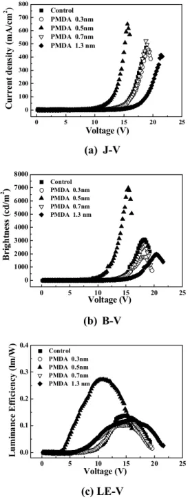
0 5 10 15 20 25 0 100 200 300 400 500 600 700 800 Control PMDA 0.3nm PMDA 0.5nm PMDA 0.7nm PMDA 1.3 nm Voltage (V) C urr en t d en si ty (m A /c m 2 ) (a) J-V 0 5 10 15 20 25 0 1000 2000 3000 4000 5000 6000 7000 8000 Control PMDA 0.3nm PMDA 0.5nm PMDA 0.7nm PMDA 1.3 nm Voltage (V) Bri ght nes s ( cd/ m 2 ) (b) B-V 0 5 10 15 20 25 0.0 0.1 0.2 0.3 0.4 Control PMDA 0.3nm PMDA 0.5nm PMDA 0.7nm PMDA 1.3 nm Voltage (V) Lu m ina nc e E ff ici en cy ( lm /W ) (c) LE-V
Figure 2. (a) J-V, (b) B-V, and (c) LE-V characteristics of the fabricated OLED devices as a function of the PMDA thickness
Figs. 2(a), (b) and (c) show the current density, brightness, and luminance efficiency characteristics of the OLED devices having the PMDA cathode interfacial layer with various thicknesses. Compared to the control sample without any cathode interfacial layer, the OLED performance was systematically improved by increasing the thickness of the PMDA layer. The best performance was achieved by using a 0.5 nm-thick PMDA layer; the turn-on voltage was reduced by ~ 6 V and the maximum brightness was increased by ~ 4,000 cd/m2. Especially, the maximum
luminance efficiency was almost doubled by using a PMDA layer with an optimum thickness. However, when the thickness of the PMDA layer was increased over 0.5 nm, the electrical and optical characteristics of the OLEDs were significantly deteriorated because the PMDA layer started to act as an insulating layer.
4. Summary
In summary, we investigated the electrical and optical characteristics of the OLEDs as a function of the thickness of the PMDA cathode interfacial layer. The OLEDs with the 0.5 nm-thick PMDA cathode interfacial layer exhibited the most performance improvement compared to the control device without any interfacial layer.
5. References
1. S. Y. Park, C. H. Lee, W.J. Song, C. Seoul, Current
Applied Physics, 1, 116 (2001).
2. X. J. Wang, J. M. Zhao, Y. C. Zhou, X. Z. Wang, S. T. Zhang, Y. Q. Zhan, Z. Xu, H. J. Ding, G. Y. Zhong, H. Z. Shi, Z. H. Xiong, Y. Liu, Z. J. Wang, E. G. Obbard, X. M. Ding, W. Huang, X. Y. Hou, J.