11-1 / N. Hirai
IMID 2009 DIGEST • A flexible OTFT-OLED display
using solution-processed organic dielectrics
Nobukazu Hirai*, Mao Katsuhara*, Iwao Yagi*, Ryoichi Yasuda*, Shin-ich Ushikura*
Makoto Noda*, Toshiki Moriwaki*, Ayaka Imaoka*, Nobuhide Yoneya*, Akira Yumoto**
Kazumasa Nomoto* and Tetsuo Urabe**
*Organic Electronics Research Laboratory, Advanced Materials Laboratories, Sony Corporation 4-16-1 Okata, Atsugi-shi, Kanagawa, 243-0021, Japan
Tel.: 81-46-226-2209, E-mail: [email protected]
**Display Device Development Group, Sony Corporation 4-14-1 Asahi-cho, Atsugi-shi, Kanagawa, 243-0014, Japan
Keywords: OTFT, OLED, Flexible Display
Abstract
We have developed a flexible OTFT backplane in which all the dielectrics are formed by solution-process in order to achieve low-cost and high-throughput manufacturing. The backplane successfully drives a flexible AM-OLED display with peak brightness of > 200 nit and the contrast ratio of > 1000:1 with great mechanical flexibility.
1. Introduction
Organic thin-film transistors (OTFTs) have been attracting increasing attention [1], because OTFTs can be flexible, lightweight and mechanically robust in comparison to conventional inorganic TFTs. These features are reflected by the properties of organic materials applied to OTFTs [2-5].
In addition, organic materials are dissolvable and their typical processing/curing temperature is below 200°C, indicating that flexible and lightweight OTFTs can be fabricated using solution-based process such as coating and printing [8] at lower temperature. Such fabrication methods lead to low-cost and high-throughput manufacturing of flexible devices using OTFTs.
Flexible displays and e-papers have been studied as potential applications of OTFTs [6-15]. Among them, a flexible OLED display driven by OTFTs (OTFT-OLED) [10-15] is a candidate for future flexible displays because of their flexibility and display properties such as fast response, clear contrast, wide color gamut, and wide viewing angle.
In this presentation, we would like to demonstrate fabrication of a flexible OTFT backplane in which all the insulation layers are formed by solution-process. An OTFT-OLED display has been successfully driven
by the backplane. Operational and mechanical stabilities of the display will be discussed.
2. Structure of our OTFT-OLED display
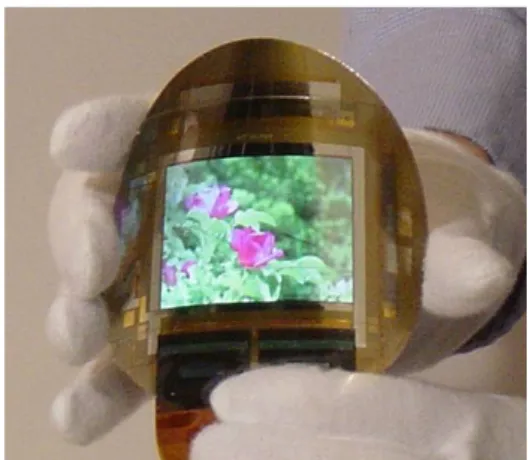
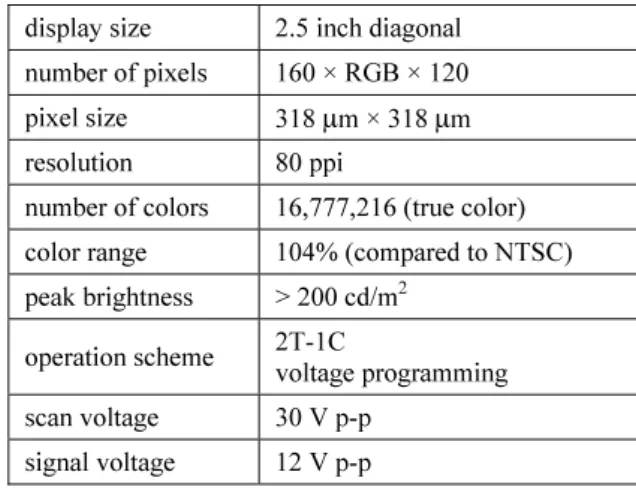
Figure 1 shows a typical photograph of our OTFT-OLED display fabricated on a flexible substrate. Specifications of the display are summarized in Table 1.
A schematic cross section of the pixel in our display is illustrated in Fig. 2. We employ a top-emission pixel structure, where OLED layers are formed onto the OTFT backplane.
11-1 / N. Hirai
• IMID 2009 DIGEST
TABLE 1. Specifications of the display
display size 2.5 inch diagonal number of pixels 160 × RGB × 120 pixel size 318 μm × 318 μm
resolution 80 ppi
number of colors 16,777,216 (true color) color range 104% (compared to NTSC) peak brightness > 200 cd/m2
operation scheme 2T-1C voltage programming scan voltage 30 V p-p
signal voltage 12 V p-p
The OTFT backplane lies between the substrate and pixel separators, in which 2T-1C pixel circuits are constructed. The backplane consists of eight patterned layers, and each layer is patterned by photolithography. A maximum temperature of 150°C is required for fabricating the backplane.
The backplane is composed of metal, organic semiconductor (OSC) and dielectric layers. Both the metal and the OSC layers are deposited in vacuum and patterned by photolithography. We apply a pentacene film to the OSC layer. All the dielectric layers in the backplane are made of organic insulators. This makes it possible to fabricate all the dielectric layers by solution processes.
3. Organic dielectrics in the OTFT backplane
In this section, organic dielectrics used in our
OTFT backplane will be discussed.
3-1. Buffer layer
Generally, surface roughness of conventional flexible substrates is not comparable to that of a glass substrate. This requires that surface roughness of the flexible substrates should be reduced before integrating OTFTs.
We coated the substrate with a solution-processed organic buffer layer in order to improve the substrate roughness. Planarization effect of solution-processed film is stronger than that of vacuum-processed one because leveling effect of solvents promotes planarization. Consequently, a peak-to-peak roughness less than 10 nm can be achieved after coating the buffer layer.
The material used for the buffer layer was carefully chosen. The buffer layer has these features. (1) It was formed below 150°C, which contributed to reduce distortion of the substrate. (2) It improved adhesion of the first metal layer.
3-2. Gate insulator
Current on/off ratio of the pixel OTFTs within a certain range of the signal voltage determines display properties such as peak brightness and contrast ratio. The current on/off ratio of an OTFT is affected by field-effect mobility and subthreshold swing (S. S.). These parameters are influenced by the interfacial trap state at OSC/gate insulator.
We apply an originally-developed organic material to the gate insulator. It was formed by spin-coating a solution of poly(4-vinyl phenol) (PVP) and octadecyltrichlorosilane (OTS). The curing temperature of this gate insulator is 150°C.
Compared to conventional PVP gate insulator, this gate insulator improves both mobility and S. S. due to the reduction of the interfacial trap state [16]. The improved OTFT shows the transfer characteristics enough to achieve peak brightness over 200 nit with a contrast ratio greater than 1000:1.
3-3. Passivation and planarization layers
The OSC layer, a pentacene film, is fragile against the exposure of common solvents [17]. In addition, recent report suggested that water affected the stability
11-1 / N. Hirai
IMID 2009 DIGEST •
of pentacene TFTs [14]. Therefore the PSV layer should protect the OSC layer from water diffusion which implies that hydrophobic materials are preferable to the PSV.
CVD of hydrophobic polymer, poly(p-xylylene) (PPX), can be one solution of non-damage passivation of a OSC layer because this is a dry process and does not require any solvents. Formation of a solution-processed planarization (PLN) layer on the PSV layer gave little damage to OTFTs. This indicates that PPX has enough chemical resistance against organic solvents as well as water used for the integration (Fig. 3(a)).
Some previous works have reported formation of a PSV layer using a water-soluble hydrophilic polymer, poly(vinyl alcohol) (PVA). Because water could degrade OTFTs, we consider that hydrophilic material is not suitable for a PSV layer and we chose here a hydrophobic amorphous polymer as a PSV layer. The polymer is solution-processed, and its curing temperature is below 100°C.
Figure 3(b) shows evolution of on currents of the pixel OTFT after the formation of solution-processed PSV and PLN layers. The degree of the reduction of on current is comparable to that of the OTFT using PPX dry passivation (Fig. 3(a)).
Figure 4 shows transfer characteristics of the pixel OTFTs after the complete integration of the backplane. The solid and dashed lines are for OTFTs using dry PPX passivation and solution-processed polymer passivation, respectively. There is no significant difference between them, indicating that the PSV layer can be solution-processed without spoiling OTFT characteristics.
3-4. Planarization layer and pixel separator
Photo-patternable organic insulators are applied to both the PLN layer and the pixel separators. The organic materials enable these layers to be formed by a simplified process with coating, direct photo-patterning, and curing.
4. Stability of the OTFT-OLED display using solution-processed organic insulators
We fabricated an OTFT-OLED display with an OTFT backplane in which all the insulation layers are formed by solution-processes
The display has been continuously operated over 8 hours with cyclic bend-and-stretch motion in every 30 seconds. Minimum bending radius is about 4 cm. The display experienced totally over 1,000-times bending after the operation test.
VGS [V] -ID [A ] VDS = -12 V CVD coating -30 -20 -10 0 10 20 10-14 10-13 10-12 10-11 1010-10 -9 10-8 10-7 10-6 10-5
Fig. 4. Comparison of OTFT properties using different passivation materials. as d ep os iti on af te r P S V & P LN as d ep os iti on af te r P S V & P LN 0.2 0.4 0.6 0.8 1.0 0 No rm ali ze d O N Cu rre nt (a) CVD grown PSV 0.2 0.4 0.6 0.8 1.0 0 (b) Solution-processed PSV No rm ali ze d O N Cu rre nt as T FT Process Step af te r P LN Process Step as T FT af te r P LN as d ep os iti on af te r P S V & P LN as d ep os iti on af te r P S V & P LN 0.2 0.4 0.6 0.8 1.0 0 No rm ali ze d O N Cu rre nt (a) CVD grown PSV 0.2 0.4 0.6 0.8 1.0 0 (b) Solution-processed PSV No rm ali ze d O N Cu rre nt as T FT Process Step af te r P LN Process Step as T FT af te r P LN as d ep os iti on af te r P S V & P LN as d ep os iti on af te r P S V & P LN 0.2 0.4 0.6 0.8 1.0 0 No rm ali ze d O N Cu rre nt (a) CVD grown PSV 0.2 0.4 0.6 0.8 1.0 0 (b) Solution-processed PSV No rm ali ze d O N Cu rre nt as T FT Process Step af te r P LN Process Step as T FT af te r P LN
Fig. 3. Evolution of on current of the pixel OTFTs during integration.
11-1 / N. Hirai
• IMID 2009 DIGEST
Figure 5 shows gamma curves, a relationship between panel brightness and the signal voltage, of the display before and after the test. The solid and dashed lines correspond to the curves before and after the test, respectively. The dashed line is shifted by a value of the threshold voltage shift (ΔVth) of OTFTs. It should be addressed here that the observed ΔVth is below 1 V for 8 hours, which is comparable to that of the panel using PPX passivation. These two lines are well overlapped, indicating that degradation of transconductance of OTFTs and efficiency of OLED did not occur during the operational test. We have also confirmed that no mechanical failure occurred after the test.
5. Conclusions
In this paper, we have shown integration of a flexible OTFT backplane in which all the insulation layers are formed by solution-process. The backplane successfully has driven top-emission OLED. The OTFT-OLED display using the backplane exhibits peak brightness over 200 nit with a contrast ratio greater than 1000:1. Mechanical and electrical stabilities of the display have been examined by a continuous operation test with a cyclic bending over 8 hours, and no intrinsic degradation is observed after the test.
6. References
1. C. D. Dimitrakopoulos and P. R. L. Malenfant,
Adv. Mater., 14, 99 (2002).
2. H. Klauk et al., J. Appl. Phys., 92, 5259 (2002). 3. Y. Kato et al., Appl. Phys. Lett., 84, 3789 (2004). 4. I. Kymissis et al., J. Vac. Sci. Technol. B,20, 956
(2002).
5. C. D. Sheraw et al., Appl. Phys. Lett., 80, 1088 (2002).
6. G.H.Gelinck et al., SID 2005 Digest of Tech. Papers, 36, 6 (2005).
7. S. E. Burns et al., SID 2006 Digest of Tech. Papers, 37, 74 (2006).
8. T. Okubo et al., Proc. Int. Display Workshops
(IDW’07), 463 (2007).
9. N. Kawashima et al., SID 2009 Digest of Tech. Papers, 40, 25 (2009).
10. M. Mizukami et al., IEEE Electron Device Lett., 27, 249 (2006).
11. L. Zhou et al., Appl. Phys. Lett., 88, 083502 (2006).
12. I. Yagi et al., SID Symposium Digest Tech. Papers, 38, 1753 (2007).
13. M. Katsuhara et al., SID Symposium Digest Tech. Papers, 40, 465 (2009).
14. S. Tokito, ECS Trans., 16, 23 (2008).
15. Y. Nakajima et al., J. Soc. Inf. Display, 17, 629 (2009).
16. N. Yoneya et al., SID Symposium Digest Tech. Papers, 37, 123 (2006).
17. D. J. Gundlach et al., Appl. Phys. Lett., 74, 3302 (1999). Signal [%]
Lu
mi
na
nc
e [
cd
/m
2]
0 20 40 60 80 100 0 100 200Fig. 5. Luminance characteristics of the panel measured before (solid line) and after (dashed line) the continuous operation.