Photogenerated plasmons in
S. YoonM. J. Seong, B. Fluegel, and A. MascarenhasS. Tixier and T. Tiedje
Citation: Appl. Phys. Lett. 91, 082101 (2007); doi: 10.1063/1.2770760 View online: http://dx.doi.org/10.1063/1.2770760
View Table of Contents: http://aip.scitation.org/toc/apl/91/8 Published by the American Institute of Physics
Photogenerated plasmons in GaAs
1−xBi
x S. YoonNational Renewable Energy Laboratory, 1617 Cole Blvd, Golden, Colorado 80401 and Division of Nano Sciences, Department of Physics, Ewha Womans University, Seoul 120-750, Korea
M. J. Seong,a兲B. Fluegel,b兲and A. Mascarenhas
National Renewable Energy Laboratory, 1617 Cole Blvd, Golden, Colorado 80401 S. Tixier and T. Tiedje
Department of Physics and Astronomy, University of British Columbia, Vancouver, British Columbia V6T 1Z1, Canada
共Received 17 May 2007; accepted 20 June 2007; published online 20 August 2007兲
Light scattering measurements in the dilute isoelectronically doped alloy GaAs1−xBixreveal a large
free electron population photogenerated by continuous-wave laser excitation at low temperature. Low-temperature time-resolved photoluminescence of the bismuth related near-band-gap states show carrier lifetimes of several nanoseconds. The authors attribute this to trapping of photoexcited holes at bismuth pair or cluster states located near the valence band maximum. © 2007 American Institute of Physics. 关DOI:10.1063/1.2770760兴
The need for semiconductor materials lattice matched to GaAs with band gap energies in the near-infrared spectral range has been growing due to the rapid progress in optical communications and photovoltaic technologies. Recently, isoelectronically doped GaAs1−xNx, for which the band gap
can be changed significantly by just a few percent of nitro-gen doping, has been studied intensely for the above appli-cations, but the reduced electron mobility fundamentally lim-its lim-its use for practical devices.1 GaAs1−xBix is a more
promising alloy material in this regard because it also exhib-its a giant band gap lowering with Bi doping;2however, the Bi incorporation is calculated to mainly perturb the valence band,3 thus holding promise for better device performance.
Spectroscopic studies2,4,5have explored the effect of Bi on the host band structure, but there has been little experi-mental work on the nature of the Bi-related states expected to occur near the band extrema. From an applications point of view, recent results6 showing good electron mobility in GaAsBi are extremely encouraging, but leave open questions about the occupation of Bi-related states by photocreated electrons and holes. Light scattering is a useful tool for this, as there are particular signatures that identify a mobile car-rier population共plasma兲. Together with time-resolved lumi-nescence, we show that hole trapping at Bi pair and cluster states results in an unusually long low-temperature lifetime and a large steady-state electron population under continuous wave共cw兲 excitation.
The samples used in our study are 0.2– 0.3-m-thick GaAs1−xBix layers共x=0.4%, 0.8%, 1.4%, and 3.1%兲 grown
by molecular beam epitaxy on共001兲 GaAs substrates. Details on the growth conditions can be found in Ref.7. Tempera-ture dependent Raman spectra and photoluminescence共PL兲 spectra were measured in a pseudobackscattering geometry using a triple spectrometer equipped with a nitrogen-cooled charge coupled device 共CCD兲 detector. The samples were excited with various powers using a using a dye laser
共190–1.93 eV兲. The spectra were obtained in the configura-tion共EiEs兲=共YY兲, where Eiand Esare the incident and
scat-tered electric field polarizations, respectively, and Y is the 关110兴 crystal direction. For zinc blende structure crystals, in the 共YY兲 scattering geometry, the longitudinal optic 共LO兲 phonon is Raman active but the transverse optic共TO兲 pho-non is not. PL was time resolved using a streak camera. Samples were excited with a 2 MHz pulse train selected from a 100 fs, 800 nm Ti:sapphire laser. 80 pJ was focused to a spot diameter of 35m.
Figure1illustrates 8 K combined PL and Raman spectra of GaAs1−xBixfor x = 0% and 1.4%. The signal from undoped
GaAs 共lower curve兲 exhibits a broad PL peak at 1.874 eV due to hot carriers recombining at the spin-orbit split off valence to conduction band transition E0+⌬0. This PL peak
is very close to the value of the E0+⌬0 transition energy previously measured at 4.2 K.8The zone center LO phonon and the very weak forbidden TO are also seen as sharp
fea-a兲Present address: Department of Physics, Chung-Ang University, Seoul, Korea.
b兲Electronic mail: brianគ[email protected]
FIG. 1. 共Color online兲 Emission spectra of GaAs and GaAs0.986Bi0.014, measured in the共YY兲 scattering geometry at 8 K. The excitation energy was adjusted for E0+⌬0 resonance in both cases, 1.901 eV for GaAs and 1.909 eV for GaAs1−xBix. The same features are also seen in the x = 0.8%
and 3.1% samples. Note that the apparent PL peak positions are modified by their different excitation energies.
APPLIED PHYSICS LETTERS 91, 082101共2007兲
tures. The upper curve shows that the addition of 1.4% Bi to GaAs results in several dramatic changes. The E0+⌬0PL is
more intense, broader, and the absolute energy of its peak has dropped by 12 meV, a combined effect of the bismuth-induced band gap reduction2 and increase in the spin-orbit splitting.5 There are also two features, L+and L−, observed above and below the LO phonon energies which have the same polarization selection as the LO phonon. These are the upper and lower branches of the coupled modes, or coupled plasmon-LO phonon modes共CPLOMs兲, between the photo-excited plasma and the LO phonon. CPLOMs in doped GaAs have a well-defined frequency that is a function of the elec-tron density, and thus serve as a direct probe of the free carrier density. Their observation in isoelectronically doped GaAsBi is unexpected, since normally an electron-hole plasma excited by a cw laser is not observed from undoped GaAs, unless the GaAs is buried below AlxGa1−xAs.
9
In fact, it has been shown that a very small surface recombination velocity is needed for the photoexcited共by a cw laser兲 plas-mon to be observed in an undoped semiconductor.10 Thus, there needs to be a mechanism, such as an electronic state which can trap photoexcited carriers, to modify the recombi-nation of electrons and holes to explain the observation of CPLOMs in GaAsBi. We will show below that the Bi pairs and cluster states located above the valence band maximum serve as traps for the photogenerated holes which hinder the recombination of the photoexcited carriers, allowing for the observation of the electron plasma in GaAsBi.
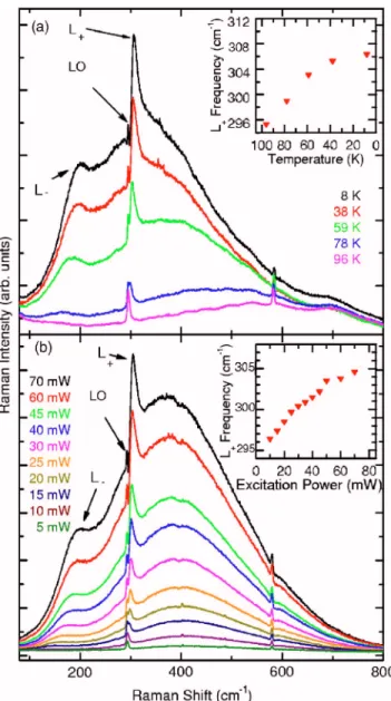
Figure2shows the results of varying this plasma density through the temperature dependence and the excitation power dependence of Raman spectra for GaAs0.986Bi0.014. Both the L+and the L−are being suppressed in intensity and
redshifted in frequency with either increasing temperature or decreasing excitation power. In particular, the L+ mode
merges toward the LO phonon at temperatures over 96 K or at excitation powers below 5 mW. The frequency shifts of the L+ mode are shown as insets in each figure. The power
dependence can be easily understood from the nature of the plasma in GaAsBi. Since the plasma is due not to charged dopants, but rather from photoexcited carriers, higher excita-tion power generates more carriers which lead to higher in-tensity and frequency of the plasmon. The temperature de-pendence, however, is not so straightforward and in fact runs opposite to the normally expected dependence for thermally generated intrinsic carriers. We believe that this peculiar tem-perature dependence is associated directly with the influence of Bi-related electronic states. Because bismuth is less elec-tronegative than the arsenic atom it replaces, it is a potential minima for holes, and thus the Bi and Bi cluster states are energetically located close to the valence band maximum 共VBM兲. The isolated Bi atom had been predicted to form a bound state;11however, a recent calculation3using larger su-percells and more extensive analysis of the origin of the VBM concluded that the isolated Bi state is actually resonant in the valence band. This leaves the possibility that Bi pairs or clusters form potential wells deep enough to bind exci-tons. Experimentally, below-band-gap transistions are indeed observed in low-temperature PL of GaAsBi,12 showing en-ergy spacing and saturation behavior that are consistent with the expected Bi cluster states. At low-to-midexcitation den-sity they dominate the PL. It is possible that at low tempera-ture, holes are trapped at these sites, thus lowering the rate of electron-hole recombination. Equivalently, the spatially
lo-calized Bi states are composed of wave functions from mul-tiple wave vector points in the valence band, which gives them a non-⌫ character, reducing their wave function overlap with the free electrons.
To test this hypothesis, we have measured time-resolved PL spectra from GaAs0.996Bi0.004in two energy ranges: first, near the E0+⌬0 transition energy using a 1.984 eV pump
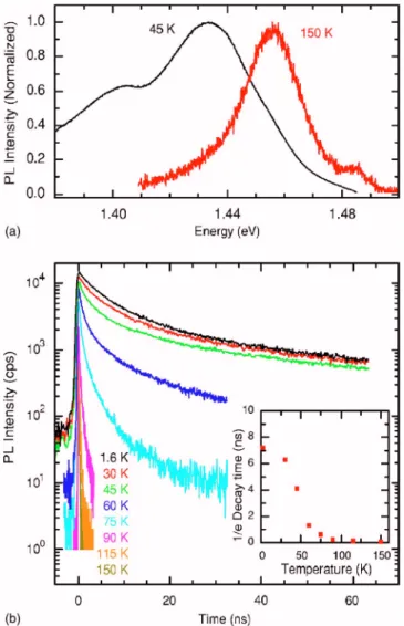
beam and next, the below-band-gap region using a 1.550 eV pump beam. Figure3共a兲shows the time-integrated PL spec-tra near 1.44 eV. At 150 K, the PL is emitted at the Bi-lowered band gap at 1.46 eV, whereas at 45 K the below-band-gap Bi-related states dominate. The PL near 1.87 eV 共shown in Fig.1兲 decays very rapidly 共not shown兲, almost as
fast as the pump beam itself, at all temperatures measured, indicating that it originates from higher-lying well-defined host band edge states where carriers are undergoing rapid relaxation. Near 1.5 eV, PL from the low-temperature GaAs FIG. 2.共Color online兲 共a兲 Raman spectra for GaAs0.986Bi0.014with an exci-tation energy of 1.901 eV at 40 mW at temperatures from 8 K共largest spec-trum兲 to 96 K 共smallest spectrum兲. All the spectra were taken in the 共YY兲 geometry. Inset: Frequency of L+mode as a function of decreasing tempera-ture.共b兲 Raman spectra for GaAs0.986Bi0.014at 10 K with an excitation en-ergy of 1.909 eV and excitation powers of 5 mW共smallest spectrum兲 to 70 mW共largest spectrum兲. Inset: frequency of L+mode as a function of excitation power. Similar temperature and power dependencies are seen in the x = 0.8% and 3.1% samples.
buffer layer decayed exponentially in 180 ps, as expected. However, the GaAsBi band edge and below-band-edge PL shown in Fig. 3共a兲 exhibit quite different behaviors. As shown in Fig.3共b兲 at temperatures starting from 90 K and above, this PL decays very rapidly, similar to GaAs, but at lower temperature, it exhibits an extraordinarily long life-time. Nearly identical time decays were also measured for the maximum bismuth concentration, x = 3.1%. The long-lived Bi hole states are the likely cause of this PL lifetime and hence also of the observation of the photoexcited elec-tron plasma. In Ref.12it was shown that the sub-band-gap states, likely triplets or higher clusters in agreement with Ref. 3, ionize at approximately 50 K. The temperature de-pendence in Fig.3共b兲, showing a similar transition tempera-ture, is thus completely consistent with the behavior of the plasmon seen in Fig.2共a兲. At temperatures above this, PL is dominated by the free carriers at the bandedge, which do not have a long lifetime.
To examine this in more detail, we note that the 1.6 K PL decay in Fig. 3共b兲 is highly nonexponential, and its power dependence 共not shown兲 indicates that the radiative recombination itself is superlinear. The 1.6 K 1 / e fall times
shown in the inset of Fig. 3共b兲 will therefore underestimate the excitation density generated by the cw laser. Using the simple coupled-mode analysis in the long-wavelength limit,13 and the effective electron mass of GaAs, electron densities corresponding to the L+ and L− frequencies of
Fig.2共b兲are calculated and shown in Fig.4. The results are consistent with the CPLOM model, and electron densities are seen to be a few ⫻1017cm−3 with a small inequality between upper and lower branches that may be due to the wavelength dependence of the plasma frequency.14 In addi-tion, the clear observation of two modes, in particular, the L+ mode with a relatively sharp linewidth and the density de-pendence seen in Fig. 4, points specifically to an electron plasma with a good mobility, as these characteristics are not seen in p-doped GaAs.15,16 This strongly supports the models3,5,6of Bi achieving a technologically useful band gap reduction by modifying primarily the valence band and leav-ing the conduction band relatively unchanged.
The authors acknowledge the financial support of the Department of Energy, Office of Science, Basic Energy Sci-ences under Grant No. DE-AC36-83CH10093.
1For review, see, for example, Y. Zhang and W. Ge, J. Lumin. 85, 247 共2000兲; C. W. Tu, J. Phys.: Condens. Matter 13, 7169 共2001兲.
2S. Francoeur, M.-J. Seong, A. Mascarenhas, S. Tixier, M. Adamcyk, and T. Tiedje, Appl. Phys. Lett. 82, 3874共2003兲.
3Y. Zhang, A. Mascarenhas, and L. W. Wang, Phys. Rev. B 71, 155201 共2005兲.
4K. Oe and H. Okamato, Jpn. J. Appl. Phys., Part 2 37, L1283共1998兲. 5B. Fluegel, S. Francoeur, A. Mascarenhas, S. Tixier, E. C. Young, and T.
Tiedje, Phys. Rev. Lett. 97, 067205共2006兲.
6D. G. Cooke, F. A. Hegmann, E. C. Young, and T. Tiedje, Appl. Phys. Lett. 89, 122103共2006兲.
7S. Tixier, M. Adamcyk, T. Tiedje, S. Francoeur, A. Mascarenhas, P. Wei, and F. Schiettekatte, Appl. Phys. Lett. 82, 2245共2003兲.
8D. E. Aspnes and A. A. Studna, Phys. Rev. B 7, 4605共1973兲. 9A. Pinczuk, J. Shah, and P. A. Wolff, Phys. Rev. Lett. 47, 1487共1981兲. 10R. Cuscó, J. Ibáñez, and L. Artús, Phys. Rev. B 57, 12197共1998兲. 11A. Janotti, S. H. Wei, and S. B. Zhang, Phys. Rev. B 65, 115203共2002兲. 12S. Francoeur, Ph.D. thesis, University of Colorado, 2004; available from
13A. Mooradian and G. B. Wright, Phys. Rev. Lett. 16, 999共1966兲. 14A. Pinczuk, L. Brillson, E. Burstein, and E. Anastassakis, Phys. Rev. Lett.
27, 317共1971兲.
15D. Olego and M. Cardona, Phys. Rev. B 24, 7217共1981兲. 16R. Fukasawa and S. Perkowitz, Phys. Rev. B 50, 14119共1994兲. FIG. 3.共Color online兲 共a兲 Time-integrated PL spectra of GaAs0.996Bi0.004at
45 and 150 K. The PL was filtered to block energies above 1.46 eV, and sent to a 0.27 m spectrometer/CCD.共b兲 Decay of the entire 1.38–1.48 eV PL spectrum shown in共a兲 at temperatures from 1.6 K 共slowest decay兲 to 150 K共fastest decay兲. Inset: plot of the time for the PL intensity to reach 1 / e of its maximum value as a function of temperature.
FIG. 4. 共Color online兲 CPLOM frequencies from Fig.2共b兲 plotted as a function of the square root of the carrier density calculated by solving for roots of the total longitudinal dielectric constant. Dashed linesp,TO, and LOshow the plasma frequency and the transverse and longitudinal optic phonons.