P2-88 / Y. S. Do
IMID 2009 DIGEST •
Abstract
A LCoS micro-display using polymer dispersed liquid crystals (PDLCs) for light switching layer was fabricated. The Si backplane of SVGA (800x600) with a pixel size of 14x14 mm2 was prepared by a 0.35µm 18V CMOS process. PDLCs were filled in the gap between backplane and ITO glass by conventional vacuum filling method. The prepared panels were driven by a field sequential color (FSC) scheme at the frequency of 180Hz and were successful in modulating LED lights to show projection images. The preparation and performance of PDLC-LCoS are presented..
1. Introduction
Mobile product market has been growing with many advanced products such as smart phones, PDA, netbooks and etc. In spite of radical developments in portable electric products, these systems have limitations in size and resolution of screen for carrying large-volume contents.
Embedded projectors are considered as one of the methods to overcome these limitations in handheld products. Many groups have developed various kinds of micro-displays for embedded projectors, including digital micro-mirror devices (DMDs) [1], spatial light modulators (SLMs) [2], Liquid Crystal on Silicon (LCoS) [3], and high temperature poly-silicon (HTPS) LCDs [4]. Among them, LCoS is regarded as a promising micro-display for embedded projectors because of its excellent performance at the small size which is enough to be integrated into handheld products such as cell phones.
In addition, attention has been paid to the fabrication of devices using polymer dispersed liquid crystals (PDLCs) because of their potential application, which includes smart windows, mobile
devices, and flexible displays. PDLCs are created when micro-droplets of liquid crystal are dispersed into a polymer matrix [5-7]. The transparency of PDLCs can be altered by external electric fields. The birefringent liquid crystal droplets form light-scattering centers, and their light-scattering properties caused by the mismatch of refractive indices, can be switched on and off by applying an electric field across the film.
In this study, we describe the fabrication and performances of LCoS panels using PDLCs.
2. Results and discussion
A 0.55” PDLC-LCoS panel was developed in SVGA (800 x 600) resolution. The designed Si backplane was fabricated using the 0.35µm / high voltage (18V) CMOS technology. The backplane has 2-poly and 4-metal layers vertically. The 2-poly and lower 2-4-metal layers form the circuitry of the Si backplane chip. The upper 2 metal layers have functions of shielding lights from the external light source and reflecting lights.
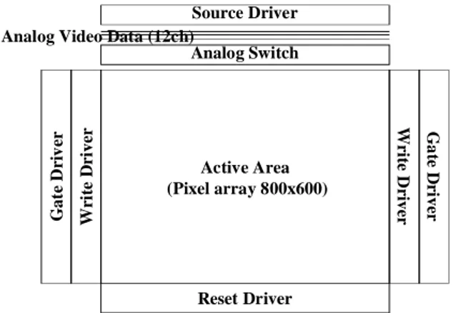
Ga te Dr iv er Wri te D ri v er Ga te D riv er W rit e D riv er Reset Driver Source Driver Analog Switch Analog Video Data (12ch)
Active Area (Pixel array 800x600)
Fig. 1. The block diagram of Si backplane chip
A 0.55” PDLC-LCoS Micro-display for Mobile Projectors
Yun Seon Do
1, Kee-Jeong Yang
1, Shi-Joon Sung
1, Jungho Kim
1, Gwang-Jun Lee
1,
Yong-Hwan Lee
1,2, Hoon-ju Chung
2, Chang-gu Roh
1,2, and Byeong-Dae Choi
1*
1
Division of Nano & Bio Technology, Daegu Gyeongbuk Institute of Science and Technology (DGIST), Daegu, 704-230, Korea
TEL:82-53-430-8410, e-mail: [email protected] 2
School of Electrical Engineering, Kumoh National Institute of Technology, Gumi, Gyeongbuk, 730-701, Korea
P2-88 / Y. S. Do
• IMID 2009 DIGEST
Fig.1 illustrates a block diagram of the LCoS backplane chip. One pixel is sized at 14 x 14 um2. The
details of the circuit were described elsewhere [8]. Both the source driver and the gate driver contain shift registers, level shifters, and buffers. For transferring 1 horizontal data, 67 times of a step is required because 12 analog video signals are transferred to the LCoS chip in parallel at the same time. The gate drivers managing each row are located on both sides to reduce the transition time. In terms of vertical driving, the shift register of the gate driver enables 600 level shifters sequentially. The reset driver has the function to refresh each pixel by erasing the previous charge which was stored at the capacitor of each pixel.
(a) (b)
Fig. 2. The PDLC-LCoS panel (a) the microscope image of PDLC film (b) the PDLC-LCoS micro display
Fig. 2 shows the LCoS panel. The LCoS panel is composed of a single Si backplane chip and ITO coated glass, and filled with a newly developed PDLC. The PDLC systems were prepared by the polymerization-induced phase separation process. The newly developed prepolymer (DG8011) consisted of a monomer, a crosslinker, and a photo initiator. A 2-ethylhexyl acrylate was used as a monomer, with 2,2-dimethoxy 2-phenylacetophenone as a photo initiator, and 1,6-hexanediol diacrylate as a crosslinker. The LC was a eutectic mixture of liquid crystals, commercially available as TL205 (Merck, Ltd.). The PDLC formulation was prepared by mixing TL205 with DG8011 homogeneously. The mixture was injected into empty LCoS cells spaced at 1µm and cured by UV irradiation. Since there doesn’t need rubbing process in the PDLC process, it is possible to reduce cost of the product compared to the conventional LCoS which is consisted with Liquid Crystal.
The transparency of PDLC is controlled by the applied voltage level between the Si backplane and the ITO glass. When the electric field is defined into the PDLC film, the birefringent liquid crystal droplets
form light-scattering centers. The mismatch of refractive indices affects the scattering properties. That makes the PDLC film to be switched ON, OFF and somewhere of the intermediate state. As a result, the PDLC-LCoS can modulate the incident lights by controlling the reflectance which is related to the scattering character.
Reflective Prism
PDLC-LCoS Panel
He-Ne Laser (633nm)
Optical Power meter 1931C (New port)
Photo detector
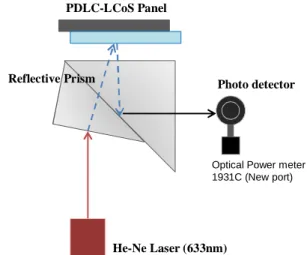
Fig. 3. Experimental setup for the measurement of reflectance of the PDLC-LCoS panel
Fig. 3 represents experimental setup for measuring the reflectance of PDLC-LCoS panel. He-Ne Laser (Melles Griot, 05-SRR-810) was used as light source. Wave length the non-polarized light source was 633nm. The reflective prism changed the direction of the light which was reflected from the PDLC-LCoS. To detect the amount of the reflected light, Optical Power meter 1931(NewPort) was used.
0 2 4 6 8 10 0 10 20 30 40 50 R e fl ec ta n ce [ % ] Voltage [Vrms] Reflectance of PDLC-LCoS
Fig. 4. Reflectance of the PDLC-LCoS panel
P2-88 / Y. S. Do
IMID 2009 DIGEST • panel as the applied voltage is increased. The range of
the applied voltage pulse is the rms value when the pulse switching at 180Hz. It reversible electric filed reduces image sticking phenomena by switching the polarity of droplets. The PDLC-LCoS panel showed the value of 12.58 as the Contrast Ratio characteristic, where it reflected 3.98% of the incident light at the OFF state and 50% at the ON state. The droplets in the PDLC film scattered light in both back and forward. Since the quantity of these both directional scattering is not equal at the steady state, a small amount of lights is reflected at the OFF state without any electric field.
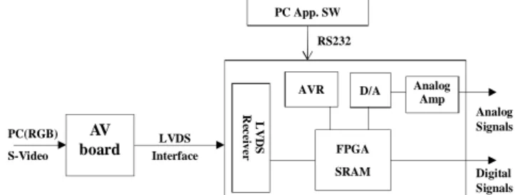
In order to drive the designed LCoS panel, 45 lines send electrical signals from the external driving board to the Si back plane. 45 pins of the chip include 12 analog video signal pins, control signal pins, and test pins for examining the chip driving state. To generate signals of 45 pins, the driving system consists of 2 blocks as shown in Fig. 5. First, the AV board does image processing. The image sources, external input video signals such as PC analog RGB, S-video, and etc., are converted to SVGA resolution in LVDS format. Second, the LCoS driver board processes the LVDS signals and generates new signals which make the Si backplane chip to work.
AV board D/A Analog Amp L VDS R ecei v e r Analog Signals FPGA SRAM Digital Signals PC App. SW AVR LVDS Interface RS232 PC(RGB) S-Video
Fig. 5. The block diagram of LCoS driving board
The programmed FPGA and SRAM build up analog and digital signals to drive the LCoS backplane circuits. Digital signals are the main sources for processing vertical and horizontal driving circuit blocks on the LCoS chips. These digital signals are synchronized by clock signals which are also derived from FPGA. The system clock goes up to 5.6 MHz to display images at a 60 Hz frame rate. The single panel system is adopted to simplify optical system and to minimize total volume of projection module. In order to separate colors, the single PDLC-LCoS panel was driven by Field Sequential Color (FSC) scheme which displays each Red, Green, and Blue color image data sequentially. Consequently, the pixels refresh the image data at 180Hz when the panel displays at 60Hz
of the frame rate.
The 12 analog video signals are sent to the LCoS panel at the same time in parallel, therefore the clock speed reduced despite of the high resolution (SVGA). The analog video signals and the analog power signals to be sent to the LCoS chip are converted from digital to analog by the 12-bit D/A convertor.
AVR block is formed in order to control driving conditions while it communicates with the PC through the RS-232 serial cable. This block related to the external PC application software allows managing timing diagram of digital control signals, frame rate, voltage levels of some analog outputs, and the γ table. This γ correction system with the 12-bit D/A convertor can express γ corrected 8-bit grayscale for each color, although the external image source and the LVDS converted image data are basically composed with linear 8-bit RGB color data.
Fig. 6. The projection image by 0.55” PDLC-LCoS panel with FSC driving scheme
The lights from R, G, and B LEDs are modulated by the PDLC-LCoS panel in which the pixel active area is 11.2 x 8.4 mm2. The image source is RGB output
from a laptop. The captured projection image using this PDLC- LCoS panel is represented in Figure 4. The image of each color was switched at 180 Hz of the sub frame rate which means 60 Hz of the frame rate. The output projection image is shown in Fig. 6.
3. Conclusion
A 0.55” SVGA LCoS micro-display was fabricated with PDLCs film for the light switching layer. The single panel system realized color image without color filters by adopting the FSC scheme while the image of each color was refreshed at 180Hz. The contrast ratio of the panel with PDLC film showed 12.58 while the panel reflected 50% of the incident lights. As a result,
P2-88 / Y. S. Do
• IMID 2009 DIGEST
the single panel system showed high luminous efficiency by producing a bright projection image. It showed the possibility of the PDLC-LCoS for the mobile display. In addition, since there is not rubbing process in the PDLC process, it is possible to produce a low-priced micro-display.
4. Acknowledgements
This work was supported by the IT R&D program of MKE / KEIT [2007-F-045-03, Developed of the projection input / output optical platform for realistic portable devices].
5. References
1. M. H. Keuper, G. Harbers, S. Paolini,SID 04 Digest,
p.943 (2004).
2. Y. Igasaki, N. Yoshida, Haruyosh, et al., Optical
review, No. 1B, p.167 (1997).
3. S. Ohuchi, T. Miyoshi, et al. ICCE. 2002 Digest of
Technical Papers, p.8 (2002).
4. M.H.Keuper, S.Paolini, G.Harbers, SID 03 Digest, p.713 (2003).
5. P.S. Drzaic, World Scientific Publishing Singapore, (1995).
6. L. Bouteiller, P.L Barny, Liq.Cryst.,21, p.157 (1996). 7. G. Spruce, R.D. Pringle, Elec. Comm. Eng. J., Elec.
Comm. Eng. J., 4, p.91 (1992).
8. H.J.Chung et al, 2nd International Conference on