P1-117 /Y. -Y. Noh
• IMID 2009 DIGEST
Abstract
Organic field-effect transistor (OFET) memory is an emerging device for its potential to realize light-weight, low cost flexible charge storage media. Here we report on a solution-processed poly[9,9-dioctylfluorenyl-2,7-diyl]-co-(bithiophene)] (F8T2) nano floating-gate memory (NFGM) with top-gate/bottom-contact device configuration. A reversible shift in the threshold voltage (VTh) and the
reliable memory characteristics were achieved by incorporation of thin Au nanoparticles (NPs) as charge storage sites for negative electrons at the interface between polystyrene and cross-linked poly(4-vinylphenol).
1. Introduction
Organic and polymeric materials are greatly attractive for individual components of many electronic devices as active semiconductors, dielectrics, and electrodes offering unique advantages over their inorganic counterparts. These materials enable deposition of uniform thin films by using simple and inexpensive solution processes. Although the organic materials are not currently suitable for electronics requiring high-end performances, the advantage in manufacturing process make them ideal for large-area, flexible, transparent, and disposable electronic devices such as organic light-emitting diodes (OLEDs),1 organic field-effect transistors
(OFETs),2 organic photovoltaic cells (OPVs).3
Organic non-volatile memories (ONVMs) are another emerging research field and one key element for the applications based on the advantages of organic
materials.4-8 Among the many possible device
configurations for organic memory, OFET-based memory is considered as a promising candidate for realization of the ultimate goal of organic flash memory because of its non-destructive read-out, complementary integrated circuit architectural compatibility, and single transistor realization.
Here we report on a solution-processed poly[9,9-dioctylfluorenyl-2,7-diyl]-co-(bithiophene)] (F8T2) NFGM with top-gate/bottom-contact (TG/BC) device configuration. By embedding Au nanoparticles (NPs) at the interface between a layer of polystyrene (PS) and a layer of cross-linked poly(4-vinylphenol) (cPVP) used as charge injection and current blocking gate dielectrics, respectively, the threshold voltage (VTh) of the polymer FET devices could be reversibly
and systemically controlled by application of external gate fields.
2. Experimental
Corning Eagle 2000 glass slides were used as substrates after cleaning sequentially in an ultrasonic bath with DI-water, acetone and iso-propanol for 10 minutes each. The chrome (adhesion layer, 5 nm) and gold (soruce/drain electrodes, 20 nm) patterns were fabricated using conventional photolithography. The patterns have channel width (W) of 1 mm and various channel lengths (L) of 2, 5, 10 and 20 µm. The semiconducting polymer, Poly[9,9-dioctylfluorenyl-2,7-diyl]-co-(bithiophene)] (F8T2) (Dow Chem.) was
Development of Highly Stable Organic Nonvolatile
Memory
Kang-Jun Baeg
1,2, Dong-Yu Kim
*,2, In-Kyu You
1and Yong-Young Noh*
,11Convergence Components & Materials Research Laboratory, Electronics
Telecommunications Research Institute (ETRI), Daejeon 305-350, Korea Tel.: 82-42-860-5633, E-mail: [email protected]
2Heeger Center for Advanced Materials, Dept. of Materials Science and Engineering,
Gwangju Institute of Science and Technology (GIST), Gwangju 500-712, Korea Tel.:82-62-970-2319, E-mail: [email protected]
P1-117 /Y. -Y. Noh
IMID 2009 DIGEST •
dissolved in anhydrous mixed xylene (10 mg/ml). Semidonductor films were fromed by a spining process and dry kept at R.T for overnight without any thermal annealing to complete remove the residual solvent in N2 purged glove box.
For fabrication of dual polymer gate dielectric layers, poly(styrene) (PS, Fluka, MW = 1,000,000) and poly(4-vinyl phenol) (PVP) (Aldrich) was used without further purification. PS and PVP solution were filtered via 0.2 µm PTFE syringe filter and spin coated onto the semiconductor. After spin coating of PS (1st dielectric layer), thin Au layer was thermal
deposited by a various thickness of 0.5, 1.0, 1.5, and 2.0 nm in a high vacuum chamber, and subsequently thermal annealed at 100 ˚C for 10 min for the formation of Au NPs. The cross-linked PVP (cPVP) layer was also spin coated onto Au deposited PS film in air, where the 1,6-bis(trichlorosilyl)hexane (C6)
(Aldrich, without purification) was used as cross-linking agent and C6 (10 µl) was mixed with base PVP
solution (1 ml). The film was annealed on hot plate at 80 ˚C for more than 1 hr to completely remove the solvents. Top-gate transistors were completed by formation of a gate electrode via thermal evaporation of aluminum films (30 nm) through a metal shadow mask.
3. Results and discussion
No positive shifts in the transfer curves of F8T2 FETs without the Au NPs were observed (Fig. 2a). By embedding of Au NPs between PS and cPVP dielectric layers, however, the transfer curves were remarkably positive shifted more than 20 V (Fig. 4b). We were verified the amount of shifts in VTh by
application of different ranges of Vg. During the Vg
sweep from 50 to -50 V, the initial transfer curves were slightly positive shifted about 7 V, but this shift did not return to its original states (no significant hysteresis behavior for using organic transistor memory). More positive shifts were taking placed during Vg sweep from 60 V to -60 V while also did
not completely recover to its initial states. The complete recovery was finally obtained by applying Vg from 70 V and -70 V that means the required
voltage for full programming and erasing in F8T2 NFGM. It should be note that the amount of positive shifts in VTh was not further increased by application
of over 70 V. This result could be explained due to limited number of charge storage sites, i.e., the number of thermally evaporated Au nano-clusters. The transfer characteristics were quietly reversible and
Fig. 1. Schematic device configuration of a TG/BC polymer field-effect transistors, and (b) chemical structure of F8T2. -80 -60 -40 -20 0 20 10-12 10-11 10-10 10-9 10-8 10-7 10-6 10-5 50 V to -50 V 70 V to -70 V 90 V to -90 V Abs I d [A ] Vg [V] At Vd = -50 V (a) -80 -60 -40 -20 0 20 10-11 10-10 10-9 10-8 10-7 10-6 10-5 Initial 50 to -50 V 60 to -60 V 70 to -70 V 80 to -80 V 90 to -90 V Abs I d [A ] Vg [V] At Vd = -50 V (b) 0.0 0.5 1.0 1.5 0 5 10 15 20 25 30 Onset Voltage Memory Window Au Thickness [nm] Onse t V o lta g e [V ] (c) 0 5 10 15 20 25 30 35 Memo ry Wind ow [V ]
Fig. 2. Transfer characteristics of F8T2 FETs, (a) without and (b) with Au 1 nm thermal evaporation. The different ranges of Vg sweeps from 50 V (-50
V) to 90 V (-90V). (c) Change of onset voltages and its amount of memory window for polymer transistor memory.
P1-117 /Y. -Y. Noh
• IMID 2009 DIGEST
systematically controlled by applying of external gate bias in a range of short time scale.
The memory window (the amount of shifts in the VTh) and the onset voltage of F8T2 FETs were linearly
increased by proportional to the amount of deposited Au NPs (Fig. 2c]. This data indicates that those reversible and controllable shifts in VTh were mainly
originated from the deposition of Au nano-clusters where the negative charge carriers were effectively trapped.
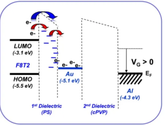
Fig. 3. Schematic demonstration of a potential operation mechanism of floating-gate F8T2 FET memory devices
The higher electric field at the PS tunnel dielectric leads efficient tunneling of negative charge carrier from the semiconductor, and trapping in Au NPs (Fig. 3). These trapped charges perturb and modulate a subsequent applied gate field resulting in substantial shifts in the VTh by the amount of equation (1);
i i i Th
C
Q
Q
d
V
=
−
=
−
∆
ε
(1)From the equation (1), we can extract that the total number of trapped charges at Au NPs is 1.5 × 1012 cm -2 at C
i = 12.2 nF/cm2 and ∆VTh = 20 V for devices
with 1 nm thick Au NPs. The calculated number of trapped charges is strongly correlated with the number density of Au NPs which was estimated by TEM images. From the rough estimation, we conclude that Au NPs of 1.25 × 1012 cm-2 are embedded between PS
and cPVP. This indicates that one electron was roughly stored in one Au NP and further electrons did not trapped in these charged Au NPs due to a repulsive force from the trapped electrons. The saturation of memory windows and the ∆VTh also
supports the trapping of one electron at one Au NP.
This result means that we have to increase the number density of Au NP to obtain larger memory window and ∆VTh.
4. Summary
The TG/BC F8T2 NFGM with a dual gate insulator has successfully demonstrated and detail operating mechanisms were discussed. The reversible shifts in VTh and reliable memory characteristics was achieved
by incorporation of thin Au NPs as a charge storage site between PS and cPVP via negative charge trapping in the Au NPs. The first report on a top-gated polymer NFGM presumably could be used as an organic transistor memory element.
Acknowledgement
This research was financially supported by the 2nd
stage Brain Korea 21 (BK21) program funded by the ministry of education, science and technology (MEST) of Korea, the national research laboratory (NRL) program of Korea science and engineering foundation (KOSEF), a grant (F0004021) from the information display R&D center one of the 21st century frontier R&D programs, development of next generation RFID technology for item level applications (2008-F052-01) funded by the ministry of knowledge economy (MKE), the program for integrated molecular systems (PIMS) at GIST.
5. References
1. K. M. Vaeth, Inform. Display, 19, 12 (2003). 2. A. Dodabalapur, Mater. Today, 9, 24 (2006). 3. M. Granström et al., Nature, 395, 257 (1998). 4. Q.-D. Ling et al., Progress in Polymer Science, 33,
917 (2008).
5. R. C. G. Naber et al., Nat. Mater., 4, 243 (2005). 6. K.-J. Baeg and D.-Y. Kim et al., Adv. Mater., 18,
3179 (2006).
7. K.-J. Baeg and D.-Y. Kim et al., Adv. Funct. Mater., 18, 3678 (2008).