heterostructures
Cite as: APL Mater. 7, 031110 (2019); https://doi.org/10.1063/1.5084201
Submitted: 05 December 2018 . Accepted: 27 February 2019 . Published Online: 25 March 2019 Hae-Yeon Lee, Sanghoon Kim , June-Young Park, Young-Wan Oh, Seung-Young Park, Wooseung Ham, Yoshinori Kotani, Tetsuya Nakamura , Motohiro Suzuki, Teruo Ono, Kyung-Jin Lee , and Byong-Guk Park
ARTICLES YOU MAY BE INTERESTED IN
Recent advances in spin-orbit torques: Moving towards device applications
Applied Physics Reviews
5, 031107 (2018);
https://doi.org/10.1063/1.5041793
Spin transfer torque devices utilizing the giant spin Hall effect of tungsten
Applied Physics Letters
101, 122404 (2012);
https://doi.org/10.1063/1.4753947
Crystal orientation dependence of spin-orbit torques in Co/Pt bilayers
Applied Physics Letters
114, 142402 (2019);
https://doi.org/10.1063/1.5090610
Enhanced spin–orbit torque via interface
engineering in Pt/CoFeB/MgO heterostructures
Cite as: APL Mater. 7, 031110 (2019);doi: 10.1063/1.5084201
Submitted: 5 December 2018 • Accepted: 27 February 2019 • Published Online: 25 March 2019
Hae-Yeon Lee,1 Sanghoon Kim,2,3,a) June-Young Park,1 Young-Wan Oh,1 Seung-Young Park,4 Wooseung Ham,3
Yoshinori Kotani,5 Tetsuya Nakamura,5 Motohiro Suzuki,5 Teruo Ono,3,6 Kyung-Jin Lee,7,8
and Byong-Guk Park1,a)
AFFILIATIONS
1Department of Materials Science and Engineering, KAIST, Daejeon 34141, South Korea 2
Department of Physics, University of Ulsan, Ulsan 44610, South Korea
3Institute for Chemical Research, Kyoto University, Uji, Kyoto 611-0011, Japan
4Spin Engineering Physics Team, Division of Scientific Instrument, KBSI, Daejeon 34133, South Korea 5Japan Synchrotron Radiation Research Institute (JASRI), Sayo, Hyogo 679-5198, Japan
6Center for Spintronics Research Network (CSRN), Graduate School of Engineering Science, Osaka University,
Osaka 560-8531, Japan
7Department of Materials Science and Engineering, Korea University, Seoul 02841, South Korea
8KU-KIST Graduate School of Converging Science and Technology, Korea University, Seoul 02841, South Korea
a)Authors to whom correspondence should be addressed:[email protected]and[email protected].
ABSTRACT
Spin–orbit torque facilitates efficient magnetisation switching via an in-plane current in perpendicularly magnetised heavy-metal/ferromagnet heterostructures. The efficiency of spin–orbit-torque-induced switching is determined by the charge-to-spin conversion arising from either bulk or interfacial spin–orbit interactions or both. Here, we demonstrate that the spin–orbit torque and the resultant switching efficiency in Pt/CoFeB systems are significantly enhanced by an interfacial modification involving Ti insertion between the Pt and CoFeB layers. Spin pumping and X-ray magnetic circular dichroism experiments reveal that this enhancement is due to an additional interface-generated spin current of the non-magnetic interface and/or improved spin transparency achieved by suppressing the proximity-induced moment in the Pt layer. Our results demonstrate that interface engineering affords an effective approach to improve spin–orbit torque and thereby magnetisation switching efficiency.
© 2019 Author(s). All article content, except where otherwise noted, is licensed under a Creative Commons Attribution (CC BY) license (http://creativecommons.org/licenses/by/4.0/).https://doi.org/10.1063/1.5084201
The electrical manipulation of magnetisation in magnetic nanostructures has opened up new avenues for the further devel-opment of spintronic devices because this approach affords sim-ple device miniaturisation and the potential for large-scale integra-tion.1–3Conventionally, spin-transfer torque (STT) has been used to control the magnetisation in magnetic multilayer structures,3,4 par-ticularly for STT-magnetic random access memory (STT-MRAM), in which a spin-polarised current is injected in the direction per-pendicular to the film plane. Recently, another type of spin-torque realised by spin–orbit coupling, the so-called spin–orbit torque (SOT),5,6has been widely investigated because it allows for efficient
manipulation of the magnetisation using in-plane current, particu-larly during magnetisation switching5,6domain-wall and skyrmion motion.7–10
SOT in heavy metal (HM)/ferromagnet (FM)/oxide het-erostructures arises from the spin current induced by a charge cur-rent via the spin Hall effect (SHE) in the HM and/or the interfacial spin–orbit coupling (ISOC) effect at HM/FM interfaces. This spin current exerts a torque T on the local magnetisation as T = τDLmˆ × (ˆy × ˆm) + τFLm × ˆy,ˆ 11,12 where τDL (τFL) denotes the damping-like torque (field-damping-like torque), ˆm denotes the unit vector along the magnetisation direction, and ˆy denotes the unit vector along the
inversion symmetry breaking (ˆz). As τDL governing SOT-induced magnetisation switching is known to arise mainly due to SHE in HMs,6,13most studies have focused on finding HM materials with a large effective spin Hall angle θeffSH14–24for the realisation of energy-efficient SOT-based spintronic devices. On the other hand, it has recently been reported that the HM/FM interface also strongly influ-ences τDL.25–33There are three examples; first, the magnitude and the sign of τDLare changed by interface modifications,26,27which is attributed to the contribution of the ISOC effect to τDL. Second, θeffSHof the HM/FM bilayer strongly depends on the spin memory loss28or the spin transparency29of its interface, thereby indicating that material engineering of HM/FM bilayers can improve the SOT efficiency. Third, the interface itself generates a spin current and thus contributes to the SOT.31,32These results suggest that interface engineering could enable further enhancement in the SOT-induced magnetisation switching efficiency.
Among various HM/FM bilayers, a Pt/CoFeB bilayer is a promising candidate for spintronic device application for the fol-lowing reasons: Pt is a highly conductive HM33 when compared with other HMs such as β-W34or β-Ta,35thus reducing Joule heat-ing and thereby power consumption.33 A CoFeB alloy is a widely used FM in spintronic devices because of its large spin polarisation in conjunction with a crystalline MgO,36and a large tunnel magne-toresistance of up to 600% at room temperature has been achieved in CoFeB/MgO-based tunnel junctions.37 Moreover, Pt/CoFeB/MgO structures have been widely used for voltage-driven spin devices, domain wall, and skyrmion motion devices.38–41However, θeff
SHof the CoFeB/Pt bilayer of 0.0725is significantly smaller than the high-est reported value among Pt/FM bilayers: ∼0.2 for Pt/Co samples;29 thus, it is of interest to further enhance the spin Hall angle in this structure.
In this study, we report significant SOT enhancement in Pt/CoFeB/MgO structures via modification of the Pt/CoFeB inter-face with the insertion of a thin Ti layer. We observe that the SOT-induced effective fields and magnetisation switching efficiency are doubled upon introducing a 1-nm-thick Ti layer at the Pt/CoFeB interface. The enhancement in SOT or θeffSHis qualitatively consistent with ferromagnetic resonance (FMR) spin-pumping experiments, in which the inverse SHE voltage of the Pt/CoFeB structure increases by twofold upon Ti insertion. Furthermore, we find that the Ti inter-facial layer markedly reduces the magnetic damping constant and the Pt proximity effect. Our results demonstrate the existence of a significant interfacial contribution and suggest that interface engi-neering can form an efficient approach to improve SOT-induced magnetisation switching.
Samples of Pt(5 nm)/Ti(tTi)/Co32Fe48B20 (CoFeB 1 nm)/ MgO(1.6 nm) structures were prepared by magnetron sputter-ing on thermally oxidised Si substrates with a base pressure of <4.0 × 10⁻⁶
Pa (3.0 × 10⁻⁸Torr) at room temperature. The Ti thick-ness tTiwas varied from 0 nm to 3 nm, and the CoFeB thickness used in this study ranged from 0.9 to 1 nm, which range guarantees strong perpendicular magnetic anisotropy (PMA). Samples were annealed at 150○
C for 40 min under vacuum conditions to induce the PMA. The Hall bar structures with a width of 5 µm were fabricated by pho-tolithography followed by Ar-ion-beam etching. All measurements were carried out at room temperature. For the spin-pumping mea-surements, the barbell-shaped samples were placed on a coplanar
quency ranging from 8 GHz to 14 GHz. The inverse spin Hall voltage VISHE was measured as a function of the external magnetic field applied along the sample plane and normal to the barbell shape.42 The soft x-ray absorption spectroscopy (XAS) at both the Co and Fe L edges was measured using the total electron yield method with the application of 96% circularly polarised incident X-rays under an applied magnetic field of 1.9 T. The X-ray propagation direction was parallel to the film normal and the 10○
-tilted magnetic field. The measurements were performed at the BL25SU beam-line at SPring8. Detailed experimental information is available in the litera-ture (including hard XMCD measurements).43,44The hard XMCD measurements were performed at the BL39XU beam-line SPring8. A transmission-type diamond X-ray phase retarder with a thickness of 1.4 mm was used to achieve a high degree of circular polarisa-tion (>95%) of X-rays. The X-ray fluorescence yield mode was used to record the X-ray absorption spectra under a magnetic field of 1.9 T. The X-ray propagation direction was parallel to the film normal and the magnetic field. During scanning around the Pt L3edge, the helicity of the X-rays was reversed at 0.5 Hz.
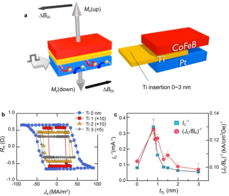
We first study the effect of the interfacial modification upon Ti insertion on SOT-induced magnetisation switching using Pt(5 nm)/Ti(tTi)/CoFeB(1 nm)/MgO Hall bar structures, where tTi is varied from 0 to 3 nm [Fig. 1(a)]. Here, we remark that Ti has a weak spin–orbit coupling42,45and that all films considered in this study have perpendicular magnetic anisotropy (PMA). To perform SOT-induced switching experiments, we sweep an in-plane current pulse with a duration of 10 µs while measuring the anomalous Hall resistance RHbetween each pulse to detect the magnetisation direc-tion. During the experiment, a magnetic field of 10 mT is applied along the current (+x) direction to achieve deterministic switch-ing.5,46Figure 1(b)shows the SOT-induced switching results, from which we can infer two points of note. One is the same switching polarity for all samples irrespective of tTi: under a positive magnetic field, positive (negative) current favours downward (upward) mag-netisation. This switching polarity corresponds to the positive θeffSHof Pt,5,46thereby indicating that the Ti insertion layer does not affect the sign of θeffSH. The second point is that the critical switching current ICreduces by half when 1 nm of Ti is inserted at the Pt/CoFeB inter-face. On the other hand, ICbecomes larger for samples with a thicker tTi, which is attributed to increase in current shunting through the Ti layer with a small θeffSH.Figure 1(c)depicts the reciprocals of the critical switching current (1/IC) and SOT switching efficiency repre-sented by the critical current density normalised by the anisotropy field (JC/Bk)−1as a function of tTi.47 This confirms that the SOT switching efficiency improves in the regime where tTilies between 0.8 and 1.5 nm. We note that the SOT switching efficiency increases by 30% with ∼1 nm-Ti insertion, indicating that the reduction in Icis substantially contributed by the decrease in Bk. Here, we con-sider that the current is uniformly distributed in the Pt/Ti bilayers since the conductivities of the Pt and the Ti layers are similar to each other, but an order of magnitude larger than that of CoFeB.22,48 The Bkvalues are in thesupplementary material. There has been a report about effect of Ta insertion between CoFeB and Pt on SOT-driven magnetization switching.48 However, unlike in our study, these authors did not show an enhancement of the SOT effect with such a heavy-metal insertion layer.
FIG. 1. (a) Schematics of spin–orbit torque (SOT)-driven
magnetisation switching (left) and the film structure (right). (b) The current-induced switching curves, anomalous Hall resistance RHvs. in-plane current density Je, according to the Ti thickness in Pt/Ti(tTi)/CoFeB/MgO(1.6 nm) structures. The values of RHare normalised for comparison (RH,Ti(0)
= 10RH,Ti(1,2) = 5RH,Ti(3)). (c) The switching efficiency of
Pt/Ti(tTi)/CoFeB/MgO (3.2 nm) structures in terms of the reciprocal of IC(left) and JC/BK(right). The error bars
rep-resent the standard deviations of the values obtained from three different samples.
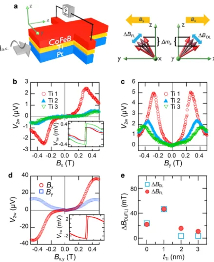
In order to quantify the effect of the Ti insertion on the SOT, we measure the SOT-induced effective magnetic fields of Pt/Ti(tTi)/CoFeB/MgO structures using the harmonic lock-in tech-nique.12,13As illustrated inFig. 2(a), the application of an ac cur-rent with a frequency of ω generates the first-harmonic Hall voltage (V1ω), which indicates the z-component of magnetisation (Mz), and the second-harmonic Hall voltage (V2ω), which represents the oscil-lation of magnetisation (∆Mz) due to SOT-induced effective fields: damping-like (∆BDL) and field-like (∆BFL) effective fields. We obtain voltages V1ω,2ωx and V1ω,2ωy when a magnetic field is applied longitu-dinally (B = Bx) and transversely (B = By) with respect to the current direction, respectively.Figures 2(b)and 2(c)display the V2ωx and Vy2ωvalues, respectively, for the Pt/Ti(tTi)/CoFeB/MgO samples with tTi= 1, 2, and 3 nm, whileFig. 2(d)presents V2ωx (closed symbols) and V2ωy (open symbols) as functions of Bx(y)for the Pt/CoFeB/MgO structures without the Ti layer for a current density Je of 1 × 10⁸A/cm2. The insets depict V1ω, which required to estimate the SOT-induced effective fields (∆BDLand ∆BFL). ∆BDLand ∆BFL values for all samples are obtained using both the 1st and the 2nd harmonic data with the narrow field regime method (from −100 to 100 mT) which has been suggested by Kim, et al.11Here, planar Hall effect and thermal effect were also taken into consideration.12,46 From this SOT analysis, we found that the magnitudes of both ∆BDL and ∆BFLin the film with tTi= 1 nm are enhanced by a factor of 2 when compared with those of the film without Ti. This result is consistent with the trend of the switching data presented inFig. 1.
We estimate θeffSHusing the conventional spin-transfer theory: ∆BDL(0)/Je = (̵h/2e) ⋅ (θeffSH/MstCoFeB),49,6 where ∆BDL(0) repre-sents the zeroth order of ∆BDL,12 ̵h represents the reduced Planck constant, e represents the elemental charge of an electron, Ms
represents the saturation magnetisation of the CoFeB layers, and Je represents the current density. The estimated value of the inserted 1-nm-thick Ti film is 0.19 ± 0.03, which is larger than that of the Pt/CoFeB film without Ti (0.13 ± 0.01). This result is consistent with the enhancement in the switching efficiency; however, it is in con-trast to previous results,25,29 wherein θeff
SHis reported to generally decrease upon insertion of an interfacial layer of a 3d metal.
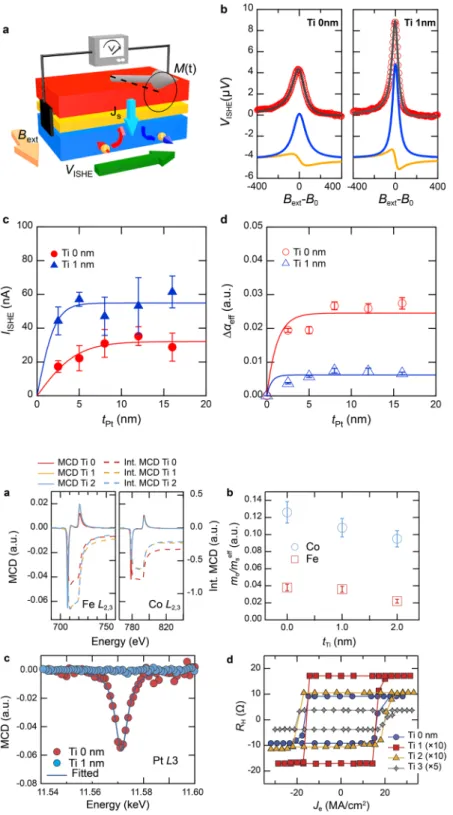
We next examine the origin of the enhancement by performing spin-pumping experiments using ferromagnetic resonance (FMR)46 for Pt (tPt)/Ti (0, 1 nm)/CoFeB/MgO films, where the Pt thickness tPt ranges from 2.5 to 16 nm. As schematically illustrated inFig. 3(a), when the magnetisation is in resonance, a spin current is injected from the CoFeB layer into the Pt layer, which leads to increase in the effective damping constant ∆αeffin the CoFeB layer along with the generation of a transverse electric voltage via inverse SHE (VISHE) in the Pt layer. The former is related to the total spin current dissipated in the CoFeB layer, while the latter is due to the spin current injected into the Pt layer. A discrepancy between the two values, ∆αeffand VISHE, can be induced if there is generation or extinction of spin current at the interface.28 The VISHEvalue is measured as a func-tion of the external magnetic field, and ∆αeffis obtained from the variation in the line width of measured VISHEspectra as a function of the FMR frequency [seeFig. 3(b)].Figures 3(c)and3(d)show the Pt thickness dependence of normalized VISHEby sample resis-tance and ∆αeff, respectively. When the 1-nm-thick Ti interfacial layer is introduced, VISHEincreases, but ∆αeffsignificantly decreases. The doubled magnitude of VISHEin the Ti-inserted samples demon-strates an increase in θeffSH of the Pt/Ti/CoFeB structure, which is consistent with the enhanced SOT shown inFigs. 1and2. More-over, the concurrent reduction in ∆αeffby insertion of 1-nm-thick Ti demonstrates that the increase in the precession angle is an origin
FIG. 2. (a) Schematic of measurement (left) and
magnetisa-tion oscillamagnetisa-tion by∆BDLand∆BFLupon applying an ac cur-rent (right). Second-harmonic Hall voltages (b) V2ω
x and (c)
V2ω
y for Pt/Ti(tTi)/CoFeB/MgO samples with different tTi val-ues. (d) V2ω
x (solid symbols) and V2ωy (open symbols) plots for the Pt/CoFeB/MgO sample. The insets in (b) and (d) depict the first-harmonic Hall voltages V1ω. (e) Damping-like effective field∆BDLand field-like effective field∆BFLas functions of tTi.
of the enhanced VISHE.50,51The decrease in ∆αeffindicates that the Ti insertion reduces a source of spin current depolarization at the Pt/CoFeB interface that is known to increase the magnetic damp-ing. While the quantitative analysis requires further study, this result suggests that the Ti insertion improves the interfacial spin trans-parency of the spin current from HM to FM and thus increase θeffSH or resultant SOT.
We next discuss the possible origins of the enhancement in θeffSHby the interfacial modification: interface-induced spin current and modified spin transparency of the FM/HM interface. We first consider the modification of the ISOC effect since the Pt/CoFeB interface is replaced by Pt/Ti and Ti/CoFeB interfaces when the Ti layer is introduced. This insertion can enhance the SOT if the ISOC effect of the Pt/CoFeB interface is of opposite sign to the bulk SHE26or if the newly generated interface of Pt/Ti provides a positive contribution.31 Here, we rule out the contribution of the Ti/CoFeB interface because our previous study showed a negligible SOT in the Ti/CoFeB/MgO structure.27To verify the modification of the ISOC effect by the Ti layer, we carry out X-ray magnetic cir-cular dichroism (XMCD) measurements at the Fe and Co L2,3edges [Fig. 4(a)]. The orbital-to-spin magnetic moment ratio (mo/mseff)
of the Pt/Ti(tTi)/CoFeB/MgO samples, which reflects the magni-tude of the ISOC effect of the HM/FM interface,52,53 is estimated using the sum rule.54,55 We find that the ratio slightly decreases with increasing tTi, thus indicating that the ISOC effect cannot be the reason for the enhanced SOT, as shown inFig. 4(b). Here, we remark that in this respect, the Pt/Ti interface can be a source of spin current and the SOT;31however, further studies are required to clarify the spin current generation from the non-magnetic interface. Another possible origin is the improvement of spin current trans-mission at interfaces which is related to the spin memory loss28or spin transparency.29As the proximity effect in Pt is a source of spin-current depolarisation, the insertion of the Ti layer may enhance the SOT by suppressing the induced moment in Pt. Thus, we investi-gate the effect of the Ti interfacial layer on the induced moment in Pt using hard XMCD analysis.Figure 4(c)shows XMCD spec-tra at the Pt L3 edges, wherein a clear XMCD signal is observed, thus indicating a finite magnetic moment induced in the Pt 5d orbit for the samples without the Ti layer; however, this signal is com-pletely eliminated by insertion of the 1-nm Ti layer. Thus, the inser-tion of the Ti layer can enhance the spin transparency and resultant SOT. We observed proximity-induced magnetic moment in the Ti insertion layer, which however is much smaller than that in the Pt
FIG. 3. (a) Schematics of the measurement. (b)
Repre-sentative VISHE values in Pt(12 nm)/Ti(0, 1 nm)/CoFeB (2 nm) structures. Symbols indicate measured data, while lines indicate fitting curves. The blue and yellow lines denote the decomposition of symmetric and anti-symmetric components, respectively. (c) VISHEnormalised by
sam-ple resistance (IISHE) vs. Pt thickness tPtfor Pt (tPt)/Ti(0, 1 nm)/CoFeB/MgO samples. (d) The effective damping constant∆αeffvs. tPtfor Pt (tPt)/Ti(0, 1 nm)/CoFeB/MgO
samples. Parameter tPt varies from 2.5 to 16 nm. The lines corresponding to VISHE and ∆αeff serve as visual
guidelines.
FIG. 4. (a) XMCD and integrated (int.) XMCD spectra at the
Fe and Co L2,3edges in the Pt/Ti (0, 1, 2 nm)/CoFeB films. (b) The orbital-to-spin magnetic moment ratio (mo/mseff) val-ues as a function of tTi. (c) Pt L3XMCD spectra of the Pt/Ti (0, 1 nm)/CoFeB/MgO films. (d) Current-induced switch-ing curves as a function of tTi for Ta/Ti(tTi)/CoFeB/MgO structures, where tTi= 0–3 nm.
layer.47 The removal of the proximity-induced moment can also explain the reduction in ∆αeffupon insertion of the Ti interfacial layer [Fig. 3(d)].56This is also supported by results indicating that the SOT monotonously decays in Ta (5 nm)/Ti(tTi)/CoFeB/MgO
structures with increase in Ti interfacial layer thickness, where the proximity effect in Ta is negligible [Fig. 4(d)].
In summary, we demonstrated a large enhancement in the SOT and SOT-induced switching efficiency in a Pt/CoFeB system
FMR spin-pumping experiments together with XMCD investiga-tions revealed that the enhancement can be attributed to an addi-tional interface-generated spin current and/or improved spin trans-parency arising due to suppression of the induced moment in the Pt layer. While a quantitative analysis of the effect of the inter-facial modification on the SOT requires further experimental and theoretical studies, our experimental results suggest that interface engineering is a promising approach to boost the efficiency of current-induced switching in SOT-based spintronic devices.
Seesupplementary material for information about the resis-tivity of each layer, anisotropy field of each film, quantitative SOT analysis, and the proximity effect in the Ti layer.
This work was supported by the National Research Foundation of Korea (Grant Nos. NRF-2015M3D1A1070465, 2017R1A2A2A05069760, and 2017M2A2A6A01071238), the Basic Research Laboratory Program through the National Research Foun-dation of Korea (NRF) funded by the MSIT (Grant No. NRF-2018R1A4A1020696), and the National Research Council of Science and Technology (NST) (Grant No. CAP-16-01-KIST). This research was also supported in part by JSPS KAKENHI Grant Nos. 26870300, 17H04924, 17H05181, 17H03377, and 15H05702 and the Center for Spintronics Research Network (CSRN). The XMCD experi-ments were performed at the SPring-8 synchrotron radiation facility with the approval of JASRI (Proposal Nos. 2017B0117, 2017B0924, 2017B0925, and 2017B0125).
REFERENCES
1I. Žuti´c, J. Fabian, and S. D. Sarma,Rev. Mod. Phys.
76, 323 (2004).
2A. Brataas, A. D. Kent, and H. Ohno,Nat. Mater.
11, 372 (2012).
3S. S. P. Parkin, M. Hayashi, and L. Thomas,Science
320, 190 (2008).
4D. Apalkov, A. Khvalkovskiy, S. Watts, V. Nikitin, X. Tang, D. Lottis, K. Moon,
X. Luo, E. Chen, A. Ong, A. D. Smith, and M. Krounbi,ACM J. Emerging Technol. Comput. Syst.9(13), 1 (2013).
5I. M. Miron, K. Garello, G. Gaudin, P.-J. Zermatten, M. V. Costache, S. Auffret,
S. Bandiera, B. Rodmacq, A. Schuhl, and P. Gambardella,Nature476, 189 (2011).
6
L. Liu, C.-F. Pai, Y. Li, H. W. Tseng, D. C. Ralph, and R. A. Buhrman,Science 336, 555 (2012).
7I. M. Miron, T. Moore, H. Szambolics, L. D. Buda-Prejbeanu, S. Auffret, B.
Rodmacq, S. Pizzini, J. Vogel, M. Bonfim, A. Schuhl, and G. Gaudin,Nat. Mater. 10, 419 (2011).
8K.-S. Ryu, L. Thomas, S.-H. Yang, and S. S. P. Parkin,Nat. Nanotechnol.
8, 527 (2013).
9
S. Emori, U. Bauer, S.-M. Ahn, E. Martinez, and G. S. Beach,Nat. Mater.12, 611 (2013).
10W. Jiang, G. Chen, K. Liu, J. Zang, S. G. E. te Velthuis, and A. Hoffmann,Phys.
Rep.704, 1 (2017).
11
J. Kim, J. Sinha, M. Hayashi, M. Yamanouchi, S. Fukami, T. Suzuki, S. Mitani, and H. Ohno,Nat. Mater.12, 240 (2013).
12K. Garello, I. M. Miron, C. O. Avci, F. Freimuth, Y. Mokrousov, S. Blügel,
S. Auffret, O. Boulle, G. Gaudin, and P. Gambardella,Nat. Nanotechnol.8, 587 (2013).
13K. Ando, S. Takahashi, K. Harii, K. Sasage, J. Ieda, S. Maekawa, and E. Saitoh,
Phys. Rev. Lett.101, 036601 (2008).
14
A. Hoffmann,IEEE Trans. Magn.49, 5172 (2013).
15
C.-F. Pai, L. Q. Liu, Y. Li, H. W. Tseng, D. C. Ralph, and R. A. Buhrman,Appl. Phys. Lett.101, 122404 (2012).
16Y. Wang, P. Deorani, X. Qiu, J. H. Kwon, and H. Yang,Appl. Phys. Lett.
105, 152412 (2014).
Lett.112, 197201 (2014).
18
B. Gu, I. Sugai, T. Ziman, G. Y. Guo, N. Nagaosa, T. Seki, K. Takanashi, and S. Maekawa,Phys. Rev. Lett.105, 216401 (2010).
19
Y. Niimi, M. Morota, D. H. Wei, C. Deranlot, M. Basletic, A. Hamzic, A. Fert, and Y. Otani,Phys. Rev. Lett.106, 126601 (2011).
20
Y. Niimi, Y. Kawanishi, D. H. Wei, C. Deranlot, H. X. Yang, M. Chshiev, T. Valet, A. Fert, and Y. Otani,Phys. Rev. Lett.109, 156602 (2012).
21
S. Woo, M. Mann, A. J. Tan, L. Caretta, and G. S. D. Beach,Appl. Phys. Lett. 105, 212404 (2014).
22
S. Cho, S.-h. C. Baek, K.-D. Lee, Y. Jo, and B.-G. Park,Sci. Rep.5, 14668 (2015).
23
K.-U. Demasius, T. Phung, W. Zhang, B. P. Hughes, S.-H. Yang, A. Kellock, W. Han, A. Pushp, and S. S. P. Parkin,Nat. Commun.7, 10644 (2016).
24J. W. Lee, Y. W. Oh, S. Y. Park, A. I. Figueroa, G. Van Der Laan, G. Go, K. J. Lee,
and B. G. Park,Phys. Rev. B96, 064405 (2017).
25
X. Fan, H. I. Çelik, J. Wu, C. Ni, K. Lee, V. O. Lorenz, and J. Q. Xiao,Nat. Commun.5, 3042 (2014).
26X. Qiu, K. Narayanapillai, Y. Wu, P. Deorani, D.-H. Yang, W.-S. Noh,
J.-H. Park, K.-J. Lee, H.-W. Lee, and H. Yang, Nat. Nanotechnol. 10, 333 (2015).
27Y.-W. Oh, S.-h. C. Baek, Y. M. Kim, H. Y. Lee, K.-D. Lee, C.-G. Yang, E.-S. Park,
K.-S. Lee, K.-W. Kim, G. Go, J.-R. Jeong, B.-C. Min, H.-W. Lee, K.-J. Lee, and B.-G. Park,Nat. Nanotechnol.11, 878 (2016).
28J.-C. Rojas-Sánchez, N. Reyren, P. Laczkowski, W. Savero, J.-P. Attané, C.
Deranlot, M. Jamet, J.-M. George, L. Vila, and H. Jaffrès,Phys. Rev. Lett.112, 106602 (2014).
29W. Zhang, W. Han, X. Jiang, S.-H. Yang, and S. S. P. Parkin,Nat. Phys.
11, 496 (2015).
30
W. Zhang, M. B. Jungfleisch, W. Jiang, Y. Liu, J. E. Pearson, S. G. E. te Velthuis, A. Hoffmann, F. Freimuth, and Y. Mokrousov,Phys. Rev. B91, 115316 (2015).
31V. P. Amin and M. D. Stiles,Phys. Rev. B
94, 104420 (2016).
32S.-h. C. Baek, V. P. Amin, Y.-W. Oh, G. Go, S.-J. Lee, M. D. Stiles, B.-G. Park,
and K.-J. Lee,Nat. Mater.17, 509 (2018).
33
M.-H. Nguyen, D. C. Ralph, and R. A. Buhrman,Phys. Rev. Lett.116, 126601 (2016).
34F. T. N. Vüllers and R. Spolenak,Thin Solid Films
577, 26 (2015).
35A. Jiang,Thin Solid Films
437, 116 (2003).
36Z. Diao, D. Apalkov, M. Pakala, Y. Ding, A. Panchula, and Y. Huai,Appl. Phys.
Lett.87, 232502 (2005).
37
S. Ikeda, J. Hayakawa, Y. Ashizawa, Y. M. Lee, K. Miura, H. Hasegawa, M. Tsunoda, F. Matsukura, and H. Ohno,Appl. Phys. Lett.93, 082508 (2008).
38K.-W. Park, J. Y. Park, S. H. C. Baek, D.-H. Kim, S.-M. Seo, S.-W. Chung, and
B.-G. Park,Appl. Phys. Lett.109, 012405 (2016).
39
R. Lo Conte, E. Martinez, A. Hrabec, A. Lamperti, T. Schulz, L. Nasi, L. Lazzarini, R. Mantovan, F. Maccherozzi, S. S. Dhesi, B. Ocker, C. H. Marrows, T. A. Moore, and M. Kläui,Phys. Rev. B91, 014433 (2015).
40
S. Woo, K. Litzius, B. Krüger, M.-Y. Im, L. Caretta, K. Richter, M. Mann, A. Krone, R. M. Reeve, M. Weigand, P. Agrawal, I. Lemesh, M.-A. Mawass, P. Fischer, M. Kläui, and G. S. D. Beach,Nat. Mater.15, 501 (2016).
41
K. Litzius, I. Lemesh, B. Krüger, P. Bassirian, L. Caretta, K. Richter, F. Büttner, K. Sato, O. A. Tretiakov, J. Förster, R. M. Reeve, M. Weigand, I. Bykova, H. Stoll, G. Schütz, G. S. D. Beach, and M. Kläui,Nat. Phys.13, 170 (2017).
42
D.-J. Kim, S.-I. Kim, S.-Y. Park, K.-D. Lee, and B.-G. Park,Curr. Appl. Phys.14, 1344 (2014).
43T. Nakamura, T. Muro, F. Z. Guo, T. Matsushita, T. Wakita, T. Hirono,
Y. Takeuchi, and K. Kobayashi,J. Electron Spectrosc. Relat. Phenom.144, 1035 (2005).
44M. Suzuki, H. Muraoka, Y. Inaba, H. Miyagawa, N. Kawamura, T. Shimatsu,
H. Maruyama, N. Ishimatsu, Y. Isohama, and Y. Sonobe,Phys. Rev. B72, 054430 (2005).
45C. Du, H. Wang, F. Yang, and P. C. Hammel,Phys. Rev. B
90, 140407 (2014).
46L. Liu, O. Lee, T. Gudmundsen, D. Ralph, and R. Buhrman,Phys. Rev. Lett.
109, 096602 (2012).
47
K.-S. Lee, S.-W. Lee, B.-C. Min, and K.-J. Lee,Appl. Phys. Lett.102, 112410 (2013).
48
P. He, X. Qiu, V. L. Zhang, Y. Wu, M. H. Kuok, and H. Yang,Adv. Electron. Mater.2, 1600210 (2016).
49
A. V. Khvalkovskiy, V. Cros, D. Apalkov, V. Nikitin, M. Krounbi, K. A. Zvezdin, A. Anane, J. Grollier, and A. Fert,Phys. Rev. B87, 020402(R) (2013).
50
O. Mosendz, J. E. Pearson, F. Y. Fradin, G. E. W. Bauer, S. D. Bader, and A. Hoffmann,Phys. Rev. Lett.104, 046601 (2010).
51
F. D. Czeschka, L. Dreher, M. S. Brandt, M. Weiler, M. Althammer, I.-M. Imort, G. Reiss, A. Thomas, W. Schoch, W. Limmer, H. Huebl, R. Gross, and S. T. B. Goennenwein,Phys. Rev. Lett.107, 046601 (2011).
52
C. Nistor, T. Balashov, J. J. Kavich, A. Lodi Rizzini, B. Ballesteros, G. Gaudin, S. Auffret, B. Rodmacq, S. S. Dhesi, and P. Gambardella,Phys. Rev. B84, 054464 (2011).
53
M. Kim, S. Kim, J. Ko, and J. Hong, Appl. Phys. Lett. 106, 102404 (2015).
54
J. T. Lau, A. Föhlisch, M. Martins, R. Nietubyc, M. Reif, and W. Wurth,New J. Phys.4, 98–101 (2002).
55
C. T. Chen, Y. U. Idzerda, H.-J. Lin, N. V. Smith, G. Meigs, E. Chaban, G. H. Ho, E. Pellegrin, and F. Sette,Phys. Rev. Lett.75, 152 (1995).
56
M. Caminale, A. Ghosh, S. Auffret, U. Ebels, K. Ollefs, F. Wilhelm, A. Rogalev, and W. E. Bailey,Phys. Rev. B94, 014414 (2016).