Importance of Purcell factor for optimizing
structure of organic light-emitting diodes
H
YUNSUC
HO,
1,4J
INC
HUNG,
2,4J
INOUKS
ONG,
2J
AEHOL
EE,
2H
YUNKOOL
EE,
1J
ONGHEEL
EE,
1,3J
AEHYUNM
OON,
1S
EUNGHYUPY
OO,
2,4ANDN
AMS
UNGC
HO1,51Flexible Device Research Group, Electronics and Telecommunications Research Institute (ETRI), 218
Gajeong-ro, Yuseong-gu, Daejeon, 34129, South Korea
2Department of Electrical Engineering, Korea Advanced Institute of Science and Technology (KAIST),
291 Daehak-ro, Yuseong-gu, Daejeon, 34141, South Korea
3Department of Creative Convergence Engineering, Hanbat National University, 125 Dongseo-daero,
Yuseong-gu, Daejeon, 34158, South Korea
4These authors have contributed equally 5[email protected]
Abstract: The ratio of spontaneous emission inside a diode structure to that in free space is called the Purcell factor (F(λ)). The structure of organic light-emitting diodes (OLEDs) has a significant influence on the spontaneous emission rate of dipole emitters. Therefore, to describe the optical properties of OLEDs, it is essential to incorporate F(λ) in the description. However, many optical studies on OLEDs continue to be conducted without considering F(λ) for simplicity’s sake. Hence, in this study, using carefully designed bottom- and top-emitting OLEDs, we show that the external quantum efficiency obtained without considering F(λ) can be over- or under-estimated, and in some cases, the margin of error may be significant. We also reveal that the subtle distribution of the electroluminescence spectrum can be explained properly only by including F(λ). Both these results stipulate the importance of including F(λ) to maintain a quantitative agreement between theoretical and experimental data. Hence, the inclusion of F(λ) is important for designing OLEDs with enhanced efficiency or desired spectral characteristics.
© 2019 Optical Society of America under the terms of the OSA Open Access Publishing Agreement
1. Introduction
To develop efficient organic light-emitting diodes (OLEDs), optical simulations are indispensable. Many researchers are interested in optical simulations and commercialized optical simulation tools have been developed [1]. These tools help in reducing the number of actual OLED fabrication and evaluation devices used for device optimization, thereby saving time and enabling a cost-effective research. In addition, optical simulations have been used to analyze experimental results [2–5]. For example, if OLED device characteristics are different from the expected results, it is possible to deduce the variables of concern. In particular, quantitative information on the dipole orientation ratios of OLED emitting materials is of high importance to predict and understand the OLED performance accurately.
Broadly, there are two typical methods in OLED optical simulations. One is based on wave optics [6–9] and the other is based on quantum electrodynamics [10–12]. In this study, we refer to the former method as “simplified model” and the latter as “full model.” In the full model, the Purcell effect is incorporated explicitly. By incorporating the Purcell effect, one can evaluate the influence of the exciton decay rate of dipole emitters in the presence of microcavity effects [13,14]. The relative enhancement of the radiative decay rate obtained under a given optical ambience ( *
rad
Γ ) over that obtained in free space (Γrad) is referred to as
#360619 https://doi.org/10.1364/OE.27.011057
the Purcell factor (F(λ)), and *
( )
rad F λ rad
Γ = Γ [10–12]. The mathematical difference due to Purcell effect in the two models will be discussed in detail in this study.
The full model gives more accurate quantitative descriptions than the simplified model because Purcell effect is considered additionally in the full model. Owing to their efficient areal uses, top-emitting OLEDs (TEOLEDs) are widely chosen in various high-resolution mobile and wearable devices (e.g., cell phones and AR or VR headsets) [15–17]. Because microcavity effect is significant in TEOLEDs, considering F(λ) is very important. Full model simulations stipulate analytical descriptions on out-coupled, substrate, waveguide, and surface plasmon polariton modes. In contrast, in simplified model simulations, only the out-coupled mode is considered. Thus, owing to the complex nature of the full model, majority of the optical analyses performed on OLEDs still adopt the simplified model for simplicity sake [18–21]. The simplified model may serve as a quick guide to predict optical characteristics, which help in understanding the OLED radiative mode distribution; however, potentially, the simplified model can misguide the description of the OLED mode distribution [22–24]. To correct the discrepancy between experimental and theoretical values, it is necessary to apply the full model in OLED analyses. In this work, we investigate the role of Purcell effect on the device characteristics of TEOLEDs and bottom-emitting OLEDs (BEOLEDs). According to our research, the simplified model yields over- or under-estimated OLED efficiency values. Our study strongly suggests the wavelength-dependent Purcell factor as an indispensable parameter to delineate the quantitative angular electroluminescence (EL) spectra accurately over a wide spectral range.
2. Optical modeling
External quantum efficiency (EQE) is a representative value indicating the performance of OLEDs. It is a typical value among optimization parameters in optical simulations. In this section, we show how Γrad and F(λ) are explicitly related to EQE. EQE is defined as the
product of the internal quantum efficiency (ηin) and the out-coupling efficiency (ηout), both of which are dependent on OLED structures [10–12]. ηin is modified by the effective radiative quantum efficiency ( *
rad
η ). As mentioned in the previous section, Γrad is not a constant value but a parameter dependent on the environment within an optical microcavity. However, nonradiative decay rate (Γnrad ) is a nonvarying term. The intrinsic radiative quantum efficiency (ηrad) is calculated as [10–12,25,26]
( )
( )
rad .rad
rad rad
nrad rad nrad rad
F F λ η η λ ∗ Γ Γ = → = Γ + Γ Γ + Γ (1) out η is defined as [10–12]
( )
( )
, out U F λ η λ = (2)where F(λ) and U(λ) are the total and out-coupled dissipated powers, respectively. The latter strongly depends on device constituting materials and their thicknesses. By adjusting F(λ) and U(λ), it is possible to deduce the optical conditions corresponding to constructive interferences for red, blue, or green color and achieve efficient OLEDs.
In a simplified model, F(λ) is assumed to be 1. This approach gives an unvarying ηin and only out-coupled power influences the EQE. If the electrical efficiency (or electron/hole balance) and singlet/triplet ratio are assumed to be 1, EQE for a simplified model (EQEsim) is
( )
.sim rad out rad
EQE =η ×η =η ×U λ (3)
Conventionally, this relation has been widely used to design and interpret OLEDs. By multiplying Eq. (1) with Eq. (2), EQE for a full model (EQEfull) is given by
( )
( )
( )
( )
( )
1 1( )
.rad
full rad out rad
nrad rad rad rad
F U EQE U F F F λ λ η η η λ λ λ η λ η ∗ Γ = × = × = × × Γ + Γ − + (4)
Moreover, it is possible to obtain the relative exciton decay lifetime ratio (τ τ λ∗ 0
( )
) inrelation to the F(λ) within a microcavity [27–29].
( )
( )
( )
( )
* 0 0 * 1 1 nrad radnrad F rad rad F rad
τ λ λ λ η λ η τ Γ + Γ Γ = = = Γ + Γ − + Γ (5)
Fig. 1. The thin film OLED structure for optical simulation (a) ITO-based bottom-emitting and (b) thin-metal-based top-emitting OLED device structures.
Not only the EQE, the spectral radiant intensity per unit area (I(λ,θ)) of the full and simplified models also differ. I(λ,θ) is commonly referred to as the enhancement factor. It is widely used to prepare a preliminary structural design and analyze the optical characteristics of OLEDs. In a simplified model, Isim(λ,θ) is given as [8]
( )
2 ( , ),( , ) , ( , ),( , ) ( , ),( , ) ( , ),( , ), sim TE TM h v TE TM h v TE TM h v TE TM h v I λ θ =A ×B ×C (6) with , , , , 3 3 3 , 0, cos , sin , 16 16 8 TE h TE v TM h e TM v e A A A θ A θ π π π = = = = (7)( )
( )
( )
( )
( )
2 2 ( , ),( , ) ( , ),( , ) ( , ),( , ) 2 ( , ),( , ) ( , ),( , ) 1 , , 1 t TE TM h v r TE TM h v TE TM h v r TE TM h v t TE TM h v t r B r r λ λ λ θ λ λ + = − (8)( )
( )
( )
3 2 ( , ),( , ) cos , , cos o o TE TM h v e e n C n λ θ λ θ λ θ = (9)where A(TE,TM),(h,v) is the dipole emission source for the type of dipole (vertical or
horizontal) and polarization (transverse electric (TE) and transverse magnetic (TM) modes) [8], B(TE,TM),(h,v) is the enhancement factor due to the interference effect, and C(TE,TM),(h,v)
corrects the differential solid angle transfer from one layer to another. The denominator in Eq. (8), called Fabry–Pérot factor, results from multiple-beam interference due to reflections between the two electrodes. The numerator is called two-beam interference factor and describes the effect of interference between the light propagating directly through a transparent electrode and that reflected from the opposite electrode in OLEDs [6,7]. The Fabry–Pérot and two-beam interference factors are also called the multibeam and wide-angle interference factors, respectively [29,30]. Optical calculations are performed by considering the optical properties (angle of incidence (θj), refractive index (nj), and thickness (dj)) of the
subdivided organic layer as shown in Fig. 1. A transfer matrix method based on the Fresnel coefficient was used to describe the interfaces in an OLED stack. rt(r) and tt(r) are the Fresnel
reflection and transmission coefficients, respectively, of an electrode. n0 and ne are the
refractive indices of the outside and emitting layers, respectively. θ0 and θe are angles of
incidence on the outside and emitting layers, respectively.
In the full model, the emissive process in OLEDs is considered to be radiating electrical dipole antennas. Chance et al. developed a theoretical framework by extending the classical electromagnetic theory of an oscillating electric dipole to the problem of molecular fluorescence in optical cavities [31,32]. The framework has been further extended to a structure where the emitter is embedded in multilayered structures [10,29,33]. The spectral radiant intensity per unit area (Iful(λ,θ)) in the full model is calculated using Eq. (10) [10],
similar to Eq. (6).
( )
2 *( )
( , ),( , ) , ( , ),( , ) ( , ),( , ) ( , ),( , ) 0 full TE TM h v TE TM h v TE TM h v TE TM h v I λ θ A B C τ λ τ = × × × (10)The difference between Eqs. (6) and (10) is the relative exciton decay lifetime, as in the case of EQE. The optical simulations were performed by custom-made MATLAB codes, and these codes were already applied in our previous studies [18,19,34]. To compare the two models, Purcell factor was set to 1 for the simplified model and to the calculated value using Eqs. (4) and (10) for the full model.
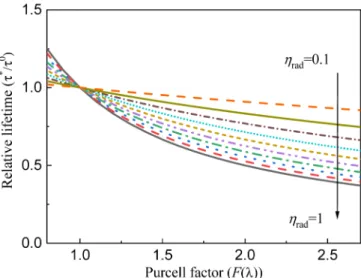
Fig. 2. The relative lifetime as a function of Purcell factor for different intrinsic quantum efficiency values.
Figure 2 shows τ τ λ∗ 0
( )
as a function of F(λ) for different values ofrad
η . If ηrad is small, τ τ λ∗ 0
( )
is not a strong function of F(λ) and does not deviate significantly from 1. ForOLED devices consisting of an emitter with a small ηradvalue, the τ τ λ∗ 0
( )
value tends tovary only about 10% from the value of 1 [35]. However, as ηrad approaches 1, τ τ λ∗ 0
( )
becomes a strong function of F(λ). As an effort to obtain high EQE OLEDs, phosphorescent and thermally activated delayed fluorescence materials are widely applied in the emissive layers [36,37]. For OLEDs using these materials, depending on the choice of F(λ), the EQE can vary upto a non-negligible value. Therefore, the Purcell factor should be considered to calculate the efficiency of OLEDs more precisely. To emphasize the significance of F(λ), we calculate it under various microcavity conditions and relate the values to the characteristics of OLED devices.
3. Experiments
The OLED structures relevant to the current work are shown in Fig. 1. To compare the effect of F(λ) on the performance of OLED devices, weak cavity ITO-based BEOLEDs were fabricated. ITO patterned glass substrates with a thickness of 70 nm were loaded into a thermal evaporation chamber after a cleaning process using sonication in a bath with acetone, isopropyl alcohol, and deionized water. 1,4,5,8,9,11-hexaazatriphenylene hexacarbonitrile (HAT-CN) and 1,1-bis ((di-4-tolylamino) phenyl) cyclohexane (TAPC) were used as hole injection and hole transporting layers, respectively. Phosphorescence green emitter tris (2-phenylpyridinato-C2,N) iridium (III) (Ir(ppy)3) doped in tris (4-carbazoyl-9-ylphenyl) amine
(TCTA) was used for a hole type host material and 2,6-bis (3-(N-carbazole) phenyl) pyridine (26DCzPPy) was used for an electron type host material. A bilayer made from these two materials forms an emission layer (EML). This bilayer EML was selected for confining excitons in a fixed region [38,39]. By using this emitter structure, it becomes possible to fix the distance between the reflective Al cathode surface and the emission zone; thus, justifying the assumption of a δ-distributed emission zone profile in numerical simulations. 1,3-bis (3,5-dipyrid-3-yl-phenyl) benzene (BmPyPB) and Li-doped BmPyPB were used as electron transporting layers (ETLs). Li-doped BmPyPB (n-ETL) enables the optical design of OLED structures without electrical losses, which may arise due to thickness and injection barrier issues. Finally, LiF and Al were deposited as a reflective cathode electrode.
To obtain strong microcavity OLEDs, it is essential to use highly reflective electrodes on both sides; hence, thin Ag-based TEOLEDs were used in this study. Instead of using an ITO film, we used a 100 nm thick Al film as a reflective anode electrode. On the Al surface, the same HTL, EML, and ETL were deposited. The top electrode consists of LiF/Al, 25 nm thick Ag film, and N,N′-Di(1-naphthyl)-N,N′-diphenyl-(1,1′-biphenyl)-4,4′-diamine (NPB) for the electron injection layer, a semitransparent electrode, and a capping layer (CL), respectively. The thicknesses of each material in the bottom- and top-emitting device structures are shown in Fig. 1.
4. Results and discussion
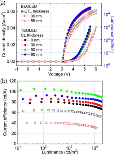
Figure 3(a) shows the current density (J), voltage (V), and luminance (L) of ITO-based BEOLEDs and thin Ag-based TEOLEDs. In a weak cavity structure, the ETL thickness was varied to change F(λ) substantially. Owing to the relatively low reflectance of ITO, the ETL thickness determines the internal optics of a given BEOLED. This thickness effectively corresponds to the spacing between the emission zone and the surface of the reflective electrode. In the case of the n-doped ETL, the J-V curves of BEOLEDs almost superimpose. However, the optically different structures have noticeable luminance differences. Thus, the variation of the OLED performance can be interpreted from the optical effect. As shown in Fig. 3(b), the devices with 30 and 55 nm n-ETL exhibited current efficiency (CE) values of
62.8 and 38.8 cd/A, respectively, at 1,000 cd/m2. This feature reflects the occurrence of
constructive interference in an OLED with a 30 nm n-ETL.
Fig. 3. (a) Current density (J), voltage (V), luminance (L), and (b) current efficiency of thin Ag-based TEOLEDs for different thicknesses of CL and ITO-based BEOLEDs for different thicknesses of Li-doped ETL.
Unlike the case of BEOLEDs, the thin Ag-based TEOLEDs were fabricated using a fixed 50 nm ETL corresponding to constructive interference for green light emission. As an alternative parameter, the CL thicknesses were variable. By varying the CL thickness, it is possible to control the reflectance and phase shift simultaneously, which take place upon reflection at the surface of the top electrode. Tuning the CL thickness to control the reflectance of the top electrode is a common method used to change the performance in TEOLEDs [40–42]. Because the CL is located outside the active layer, it does not affect the electrical characteristics of the devices. Therefore, the J-V curves of the devices superimpose despite the different CL thicknesses in the devices. Compared to the optimized BEOLEDs with a 30 nm n-ETL, TEOLEDs exhibited much higher current efficiency (Fig. 4(b)). The current efficiencies of all TEOLEDs are higher than 80 cd/A in the entire luminance range of consideration. In comparison, the highest current efficiency of the optimized BEOLED is 64 cd/A at 100 cd/m2. The current efficiencies were obtained by measuring the emissions from
the normal direction. Using a Lambertian luminance distribution, the emission direction is not considered. However, owing to the presence of microcavity, angle-resolved emission and spectra must be considered to obtain the correct OLED characteristics. Tables 1 and 2
summarize the measured and simulated EQE values of the BEOLEDs and TEOLEDs, respectively, based on the angle-resolved intensities and spectra.
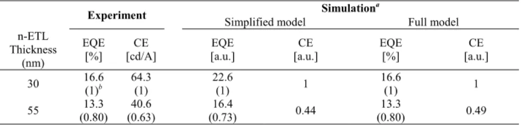
EQE values are also calculated by using the simplified and full models (refer to Tables 1 and 2). It is possible to ignore the Purcell effect by setting F(λ) = 1. However, this approach does not allow us to calculate real EQE values. Herein, we use the EQE values obtained using F(λ) = 1 to emphasize the importance of Purcell effect. ηin was adjusted such that the
simulated EQE values from the full model coincide with the measured EQE values. The ITO-based BEOLED with a 55 nm n-ETL has a lower relative efficiency value in the simplified model than that in the full model if the BEOLED with a 30 nm n-ETL is used as a reference device. The simplified model causes underestimated efficiency values compared to the full model, and the difference between them is about 10%. On the other hand, thin Ag-based TEOLEDs have higher relative efficiency values in the simplified model than those in the full model. The simplified model causes overestimated efficiency values, and the difference between two models is much larger than 10%. Especially, TEOLEDs with 0 and 90 nm CLs are estimated to have relatively larger efficiency values than 1 in the simplified model; however, those have relatively smaller efficiency than 1 in the full model. In other words, the relative efficiency values are model dependent and can be calculated inversely according to the models. Thus, in designing efficient OLEDs, one has to be very cautious in the choice of F(λ).
Table 1. Measured and Simulated EQEs and CEs of BEOLEDs Experiment Simplified model Simulationa Full model
n-ETL Thickness (nm) EQE [%] CE [cd/A] EQE [a.u.] CE [a.u.] EQE [%] CE [a.u.] 30 16.6 (1)b 64.3 (1) 22.6 (1) 1 16.6 (1) 1 55 (0.80) 13.3 (0.63) 40.6 (0.73) 16.4 0.44 (0.80) 13.3 0.49
aAssuming that internal quantum efficiency is 0.74.
bThe values in parentheses indicate the relative values considering the BEOLED with 30 nm n-ETL as reference.
Table 2. Measured and Simulated EQEs and CEs of TEOLEDs
Experiment Simulation
a
Simplified model Full model
CL thickness (nm) EQE [%] CE [cd/A] EQE [a.u.] CE [a.u.] EQE [%] CE [a.u.] 0 (0.93)15.0 b (1.26) 80.7 (1.13) 25.5 1.46 (0.76) 12.6 1.05 30 (1.01) 16.8 (1.34) 86.1 (1.35) 30.4 1.57 (1.01) 16.8 1.23 60 (1.10) 18.3 (1.63) 105.1 (1.44) 32.6 1.87 (1.11) 18.5 1.52 90 (0.93) 15.5 (1.44) 92.9 (1.23) 27.9 1.75 (0.92) 15.3 1.42
aAssuming that internal quantum efficiency is 0.8.
bThe values in parentheses indicate the relative values considering the BEOLED with 30 nm n-ETL as reference.
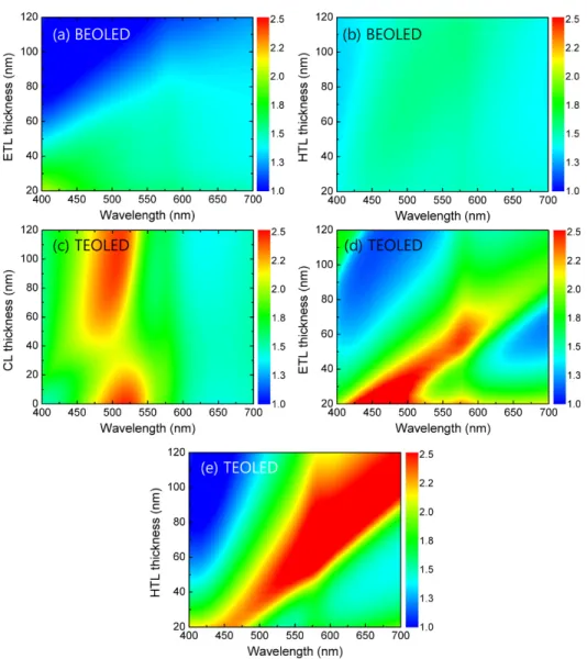
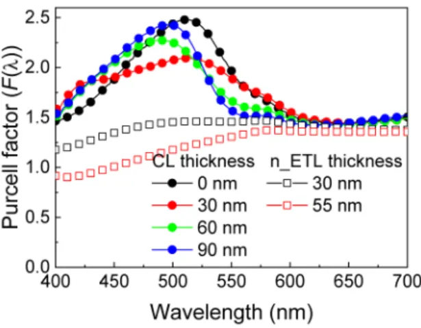
Fig. 4. The F(λ)s of ITO-based BEOLEDs for different (a) ETL and (b) HTL thicknesses and that of thin Ag-based TEOLEDs for different (c) CL, (d) ETL, and (e) HTL thicknesses.
Figures 4(a) and (b) show the dependency of the F(λ) of BEOLEDs on the thicknesses of ETL and HTL, respectively. The reflectance of the transparent electrode is not high enough to cause the interference effect in an OLED structure. Thus, the ETL thickness, i.e., the distance between the emission zone and the reflective electrode, has greater influence on F(λ) than the HTL thickness, i.e., the distance between the emission zone and the transparent electrode. Figures 4(c), 4(d), and 4(e) show the dependency of the F(λ) of TEOLEDs on CL, ETL, and HTL thicknesses, respectively. Unlike BEOLEDs, all thicknesses of CL, ETL, and HTL in TEOLEDs have a profound influence on the Purcell factor. This is due to the high reflectance of the thin metal electrodes in TEOLEDs, which induce strong interference effects. As a result, the varying CL thicknesses can affect the reflectance intensity in an interference condition, while the varying ETL or HTL thicknesses can affect the interference path length. In other words, in analyzing and designing TEOLEDs, F(λ) cannot be ignored.
Fig. 5. The F(λ)s of the BEOLEDs and TEOLEDs used in this study.
The reference device has an F(λ) of about 1.48 at a wavelength of 520 nm as shown in Fig. 5. If the thickness of the n-ETL was increased to 55 nm, F(λ) at the same wavelength decreased to 1.2, resulting in the increase of τ τ λ∗ 0
( )
from 0.74 to 0.87 (refer to Fig. 2 forηin = 0.72). In this case, the EQE calculated by using the simplified model is underestimated
compared to the value obtained from the full model because τ τ λ∗ 0
( )
is 1 in the simplifiedmodel but different in the full model. As shown in Table 1, the relative efficiency for the simplified model is 0.73, but it is 0.80 for the full model. On the other hand, regardless of the thickness of the CL, the F(λ) for all the TEOLEDs is greater than 2 at a wavelength of 520 nm, which is larger than that of the BEOLEDs as shown in Fig. 4(b). τ τ λ∗ 0
( )
of theTEOLEDs is about 0.56 (refer to Fig. 2 for ηin = 0.8), which is smaller than that of the
reference device. As a result, the calculated EQE values of the simplified model are overestimated compared to those of the full model. Here, the EQE difference may not be large, but it depends critically on the value of F(λ).
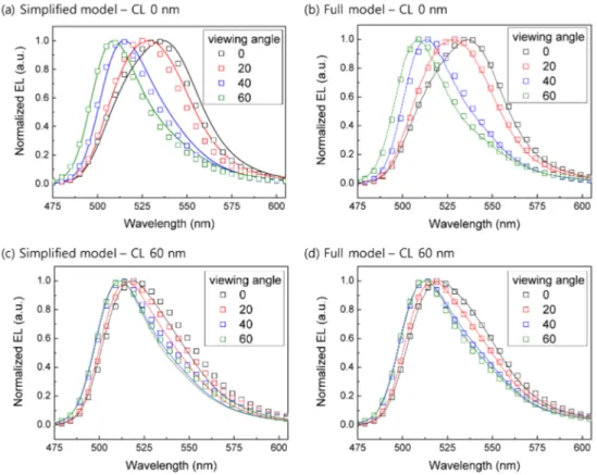
In addition, color coordinate, color purity, and angular color shift in TEOLEDs were more susceptible to the device structure than those in BEOLEDs owing to the strong resonance effect of TEOLEDs. As discussed in Section 2, the angular emission spectra are also proportional to τ τ λ∗ 0
( )
or inversely proportional to F(λ), referring to Eqs. (5) and (10).Figure 6 shows the normalized angular emission spectra of TEOLEDs without a CL and with a CL of thickness 60 nm. In the simplified model, the peak position of the calculated emission spectra is slightly away from that of the measured emission spectra, although the blue shift of the emission spectra with increasing viewing angles is the same for both the spectra. The blue shift of the emission spectra at different viewing angles can be explained by the interference effect as shown by Eq. (8). The resonance wavelength is in a cosine function relation with the viewing angle [7]. In TEOLEDs, the interference effect is not sufficient to explain the position of the emission spectra. As shown in Fig. 5, the F(λ) for BEOLEDs is a weak function of wavelength such that ignoring the Purcell effect dose not significantly change the shape of the emission spectra. However, the F(λ) for TEOLEDs rapidly changed for wavelengths ranging from 500 to 550 nm. This change of F(λ) influences the peak position of the emission spectra at each viewing angle. Hence, the calculated emission spectra in the full model are modified and they agree well with the measured emission spectra as shown in Figs. 6(b) and 6(d).
Fig. 6. Measured (represented using squares) and calculated (represented using lines) normalized angular emission spectra of TEOLEDs without a CL using (a) simplified model and (b) full model, and with a CL of thickness 60 nm using (c) simplified model and (d) full model.
5. Conclusion
In the studies so far, the Purcell effect was not considered explicitly during OLED optical simulations, potentially yielding misleading results in the performance estimation and device design of OLEDs. In this work, we demonstrated the importance of the Purcell factor by varying the OLED device structures. Results show that Purcell effect is significant in OLEDs in which high radiative quantum efficiency emissive materials are used. In such materials, the effective exciton lifetime and decay rate are strongly influenced by the Purcell factor. To verify the technical significance of Purcell factors experimentally, we fabricated actual BEOLEDs and TEOLEDs with various structures. In the case of TEOLEDs with a strong resonance structure, overestimation was avoided and more accurate optical simulation results were obtained by considering the Purcell factor. The results also show that the efficiency and angular emission spectra of the OLEDs were estimated accurately. From practical viewpoints, because many mobile AM-OLED gadgets use TEOLEDs, we believe our approach can serve as a useful guide to design efficient and angular stable EL spectra TEOLEDs.
Funding
National Research Council of Science & Technology (NST) (CMP-16-05-ETRI); Electronics and Telecommunications Research Institute (ETRI) (19ZB1220); Ministry of Trade, Industry and Energy/Korea Evaluation Institute of Industrial Technology (MOTIE/KEIT) (10044412).
References
<conf>1. S. Altazin, C. Reynaud, U. M. Mayer, T. Lanz, K. Lapagna, R. Knaack, L. Penninck, C. Kirsch, K. P. Pernstich, S. Harkema, D. Hermes, and B. Ruhstaller, “Simulations, measurements and optimization of OLEDs with scatter layer,” SID Symposium Digest 46, 564–567 (2015).</conf>
<jrn>2. B. C. Krummacher, S. Nowy, J. Frischeisen, M. Klein, and W. Brütting, “Efficiency analysis of organic light-emitting diodes based on optical simulation,” Org. Electron. 10(3), 478–485 (2009).</jrn>
<jrn>3. R. Meerheim, M. Furno, S. Hofmann, B. Lüssem, and K. Leo, “Quantification of energy loss mechanisms in organic light-emitting diodes,” Appl. Phys. Lett. 97(25), 253305 (2010).</jrn>
<jrn>4. M. Flämmich, J. Frischeisen, D. S. Setz, D. Michaelis, B. C. Krummacher, T. D. Schmidt, W. Brütting, and N. Danz, “Oriented phosphorescent emitters boost OLED efficiency,” Org. Electron. 12(10), 1663–1668 (2011).</jrn>
<jrn>5. H. Shin, S. Lee, K.-H. Kim, C.-K. Moon, S.-J. Yoo, J.-H. Lee, and J.-J. Kim, “Blue phosphorescent organic light-emitting diodes using an exciplex forming co-host with the external quantum efficiency of theoretical limit,” Adv. Mater. 26(27), 4730–4734 (2014).</jrn>
<jrn>6. D. G. Deppe, C. Lei, C. C. Lin, and D. L. Huffaker, “Spontaneous emission from planar microstructures,” J. Mod. Opt. 41(2), 325–344 (1994).</jrn>
<jrn>7. H. Cho, C. Yun, and S. Yoo, “Multilayer transparent electrode for organic light-emitting diodes: tuning its optical characteristics,” Opt. Express 18(4), 3404–3414 (2010).</jrn>
<jrn>8. H. Benisty, R. Stanley, and M. Mayer, “Method of source terms for dipole emission modification in modes of arbitrary planar structures,” J. Opt. Soc. Am. A 15(5), 1192–1201 (1998).</jrn>
<jrn>9. Z. B. Wang, M. G. Helander, X. F. Xu, D. P. Puzzo, J. Qiu, M. T. Greiner, and Z. H. Lu, “Optical design of organic light emitting diodes,” J. Appl. Phys. 109(5), 053107 (2011).</jrn>
<jrn>10. M. Furno, R. Meerheim, S. Hofmann, B. Lüssem, and K. Leo, “Efficiency and rate of spontaneous emission in organic electroluminescent devices,” Phys. Rev. B Condens. Matter Mater. Phys. 85(11), 115205 (2012).</jrn>
<jrn>11. T. D. Schmidt, B. J. Scholz, C. Mayr, and W. Brütting, “Efficiency analysis of organic light-emitting diodes based on optical simulations,” IEEE J. Sel. Top. Quantum Electron. 19(5), 1 (2013).</jrn>
<jrn>12. W. Brütting, J. Frischeisen, T. D. Schmidt, B. J. Scholz, and C. Mayr, “Device efficiency of organic light-emitting diodes: Progress by improved light outcoupling,” Phys. Status Solidi., A Appl. Mater. Sci. 210(1), 44– 65 (2013).</jrn>
<jrn>13. E. M. Purcell, “Spontaneous emission probabilities at radio frequencies,” Phys. Rev. 69, 681 (1946).</jrn>
<jrn>14. K. H. Drexhage, “Influence of a dielectric interface on fluorescence decay time,” J. Lumin. 1–2, 693–701 (1970).</jrn>
<conf>15. H.-K. Chung, H.-D. Kim, and B. Krista, “AMOLED Technology for Mobile Displays,” SID Symposium Digest 37, 1447–1450 (2006).</conf>
<conf>16. A. Ghosh, E. P. Donoghue, I. Khayrullin, T. Ali, I. Wacyk, K. Tice, F. Vazan, L. Sziklas, D. Fellowes, and R. Draper, “Directly patterned 2654 PPI full color OLED microdisplay for head mounted wearables,” SID Symposium Digest 47, 837–840 (2016).</conf>
<conf>17. U. Vogel, B. Richter, O. Hild, P. Wartenberg, K. Fehse, M. Schober, S. Brenner, J. Baumgarten, P. König, B. Beyer, G. Bunk, S. Ulbricht, C. Schmidt, M. Jahnel, E. Bodenstein, S. Saager, C. Metzner, and V. Kirchhoff, “OLED microdisplays—enabling advanced near-to-eye displays, sensors, and beyond,” SID Symposium Digest
47, 703–706 (2016).</conf>
<jrn>18. T. V. Hoang, S. E. Lee, J. G. Lee, Y. K. Kim, and J. H. Lee, “Optimum thickness of epsilon negative tri-metal layer electrodes for maximizing OLED outcoupling efficiency,” Opt. Express 25(25), 31006–31016 (2017).</jrn>
<jrn>19. are J.-X. Man, S.-J. He, D.-K. Wang, H.-N. Yang, and Z.-H. Lu, “Tailoring Mg:Ag functionalities for organic light-emitting diodes,” Org. Electron. 63, 41–46 (2018).</jrn>
<jrn>20. Y. Li, Z. Tang, C. Hänisch, P.-A. Will, M. Kovačič, J.-L. Hou, R. Scholz, K. Leo, S. Lenk, and S. Reineke, “Ultrathin MoO3 layers in composite metal electrodes: Improved optics allow highly efficient organic light-emitting diodes,” Adv. Opt. Mater. 7(3), 1801262 (2019).</jrn>
<jrn>21. M. Chakaroun, A. T. Diallo, S. Hamdad, S. Khadir, A. P. A. Fischer, and A. Boudrioua, “Experimental and theoretical study of the optical properties optimization of an OLED in a microcavity,” IEEE Trans. Electron Dev. 65(11), 1 (2018).</jrn>
<jrn>22. J. Lee, T.-H. Han, M.-H. Park, D. Y. Jung, J. Seo, H.-K. Seo, H. Cho, E. Kim, J. Chung, S.-Y. Choi, T.-S. Kim, T.-W. Lee, and S. Yoo, “Synergetic electrode architecture for efficient graphene-based flexible organic light-emitting diodes,” Nat. Commun. 7(1), 11791 (2016).</jrn>
<jrn>23. H. Cho, J. Chung, J. Lee, E. Kim, and S. Yoo, “Dual optical role of low-index injection layers for efficient polarizer-free high contrast-ratio organic light-emitting diodes,” Opt. Express 23(8), 10259–10265 (2015).</jrn> <jrn>24. H. Cho, C. W. Joo, B.-H. Kwon, N. S. Cho, and J. Lee, “Non-linear relation between emissive dipole
orientation and forward luminous efficiency of top-emitting organic light-emitting diodes,” Org. Electron. 62, 72–76 (2018).</jrn>
<jrn>25. X.-W. Chen, W. C. H. Choy, S. He, and P. C. Chui, “Comprehensive analysis and optimal design of top-emitting organic light-top-emitting devices,” J. Appl. Phys. 101(11), 113107 (2007).</jrn>
<jrn>26. S. Mladenovski, S. Reineke, and K. Neyts, “Measurement and simulation of exciton decay times in organic light-emitting devices with different layer structures,” Opt. Lett. 34(9), 1375–1377 (2009).</jrn> <jrn>27. E. F. Schubert, N. E. J. Hunt, M. Micovic, R. J. Malik, D. L. Sivco, A. Y. Cho, and G. J. Zydzik, “Highly
efficient light-emitting diodes with microcavities,” Science 265(5174), 943–945 (1994).</jrn>
<jrn>28. S. Hofmann, M. Thomschke, B. Lüssem, and K. Leo, “Top-emitting organic light-emitting diodes,” Opt. Express 19(S6 Suppl 6), A1250–A1264 (2011).</jrn>
<jrn>29. K. A. Neyts, “Simulation of light emission from thin-film microcavities,” J. Opt. Soc. Am. A 15(4), 962– 971 (1998).</jrn>
<jrn>30. S. Chen, L. Deng, J. Xie, L. Peng, L. Xie, Q. Fan, and W. Huang, “Recent developments in top-emitting organic light-emitting diodes,” Adv. Mater. 22(46), 5227–5239 (2010).</jrn>
<jrn>31. R. R. Chance, A. Prock, and R. Silbey, “Lifetime of an emitting molecule near a partially reflecting surface,” J. Chem. Phys. 60(7), 2744–2748 (1974).</jrn>
<jrn>32. R. R. Chance, A. Prock, and R. Silbey, “Molecular fluorescence and energy transfer near interfaces,” Adv. Chem. Phys. 37, 1–65 (2007).</jrn>
<jrn>33. K. G. Sullivan and D. G. Hall, “Enhancement and inhibition of electromagn etic radiation in plane-layered media. I. Plane-wave spectrum approach to modeling classical effects,” J. Opt. Soc. Am. B 14(5), 1149–1159 (1997).</jrn>
<jrn>34. J. Song, K.-H. Kim, E. Kim, C.-K. Moon, Y.-H. Kim, J.-J. Kim, and S. Yoo, “Lensfree OLEDs with over 50% external quantum efficiency via external scattering and horizontally oriented emitters,” Nat. Commun. 9(1), 3207 (2018).</jrn>
<jrn>35. R. H. Jordan, A. Dodabalapur, and R. E. Slusher, “Efficiency enhancement of microcavity organic light emitting diodes,” Appl. Phys. Lett. 69(14), 1997–1999 (1996).</jrn>
<jrn>36. K.-H. Kim and J.-J. Kim, “Origin and control of orientation of phosphorescent and TADF dyes for high-efficiency OLED,” Adv. Mater. 30(42), 1705600 (2018).</jrn>
<jrn>37. Y. Im and J. Y. Lee, “Recent progress of green thermally activated delayed fluorescent emitters,” J. Inf. Disp. 18(3), 101–117 (2017).</jrn>
<jrn>38. S.-J. Su, E. Gonmori, H. Sasabe, and J. Kido, “Highly efficient organic blue-and white-light-emitting devices having a carrier- and exciton-confining structure for reduced efficiency roll-off,” Adv. Mater. 20, 4189– 4194 (2008).</jrn>
<jrn>39. Z. Zhang, S. Yue, Y. Wu, P. Yan, Q. Wu, D. Qu, S. Liu, and Y. Zhao, “Low driving voltage blue, green, yellow, red and white organic light-emitting diodes with a simply double light-emitting structure,” Opt. Express
22(2), 1815–1823 (2014).</jrn>
<jrn>40. H. Riel, S. Karg, T. Beierlein, W. Riess, and K. Neyts, “Tuning the emission characteristics of top-emitting organic light-top-emitting devices by means of a dielectric capping layer: an experimental and theoretical study,” J. Appl. Phys. 94(8), 5290–5296 (2003).</jrn>
<jrn>41. Q. Huang, K. Walzer, M. Pfeiffer, V. Lyssenko, G. He, and K. Leo, “Highly efficient top emitting organic light-emitting diodes with organic outcoupling enhancement layers,” Appl. Phys. Lett. 88(11), 113515 (2006).</jrn>
<jrn>42. J. W. Huh, J. Moon, J. W. Lee, D.-H. Cho, J.-W. Shin, J.-H. Han, J. Hwang, C. W. Joo, J.-I. Lee, and H. Y. Chu, “The optical effects of capping layers on the performance of transparent organic light-emitting diodes,” IEEE Photonics J. 4(1), 39–47 (2012).</jrn>