A DISSERTATION
FOR THE DEGREE OF DOCTOR OF PHILOSPHY
Synthesis of Functional Nanostructured and
Nanocomposite Materials for Printed Electronic Devices
Ghayas Uddin Siddiqui
Department of Mechatronics Engineering
GRADUATE SCHOOL
JEJU NATIONAL UNIVERSITY
Synthesis of Functional Nanostructured and
Nanocomposite Materials for Printed Electronic Devices
Ghayas Uddin Siddiqui
(Supervised by Professor Kyung Hyun Choi)
A thesis submitted in partial fulfillment of the requirement for the degree of Doctor of Philosophy
2017. 06
The thesis has been examined and approved.
Thesis director, Jong-Hwan Lim, Professor, Department of Mechatronics Engineering
Yang-Hoi Doh, Professor, Department of Electronic Engineering
Chul-Ung Kang, Professor, Department of Mechatronics Engineering
Chang-Nam Kang, Professor, Department of Mechanical Engineering
Kyung-Hyun Choi, Professor, Department of Mechatronics Engineering
June 2017 Date Department of Mechatronics Engineering
GRADUATE SCHOOL JEJU NATIONAL UNIVERSITY
I
Dedicated to
II
Acknowledgments
The first and foremost gratitude to my Almighty Allah Who Bestows His Grace on me in every phase of my life and then to my beloved parents as they have continued to shower their prayers and most precious love for me even after departing the world. I miss them intensely in every step of my life and their immortal love makes me more and more strong.
I am immensely grateful to my supervisor Prof. Dr. Kyung Hyun Choi for his skillful guidance, support and confidence on me throughout my stay at Advance Micromechatronics (AMM) lab. It has been an honor for me to work under his supervision as he has always provided decent funding, accurate direction, and motivation to flourish my research.
I am very thankful to Ms. Qamar Naz and Dr. Nauman Malik for believing in me and recommending me in AMM lab. I would like to say a special thanks to my younger brother Waqas Uddin Siddiqui who managed all the family matters so nicely in my absence. An adorable gratitude to my loving sisters, sweet nephews and nieces who bless me always with their prayers and love. I am also very thankful to my uncles, aunts and cousins for their affectionate countenance even when I was unable to contact them oftenly.
I will always be grateful to my seniors in AMM lab including Dr. Maria Mustafa, Dr. Adnan Ali, Dr. Navaneethan, Dr. Muhammad Zubair, Dr. Syed Murtaza, Dr. Kamran Ali, Dr. Junaid Ali, and Dr. Shahid Aziz as I have learned a lot from them. I am fortunate enough to have Memoon Sajid, Muhammad Muqeet Rehaman, Jahanzeb Gul, J. Srikanth, Imran Shah, Muhammad Mutee ur Rehman, Shital Kumar and Muhsin Ali as my dear friends and in AMM lab as they are nothing short of amazing persons.
I am very thankful to my Korean friends and colleagues including Dr. Hyun Woo Dong, Dr. Bong Su Yang, Dr. Young Jin Yang, Go-Bum Kim, Hyeon Beom Kim, Soo Wan Kim, Young
III
Soo Kim, Hyu Tae Kim, Kyung Huwan, Jae Wook, Dae-You Kim, Ms. Jae Hee Park and Ms. Jiyun; without their assistance my stay at Jeju would not have been so comfortable and pleasant. I am really grateful to my dear friends in Jeju including Waqar Kayani Sahab, Dr. Jamil Ahmed, Dr. Farrukh Israr, Dr. Safdar Ali, Dr. Rashid Ahmed, Dr. Zahid Manzoor, Dr. Sohail khan, Dr. Shawkat Ali, Dr. Waqar Abbasi, Dr. Afaq Muhammad, Dr. Anil Kumar, Dr. Karthi Krish, Dr. Konstantin Lyakhov, Aleem Khaliq, Zubair Amjad, Irshad Ali, Waseem Abbas, Gul Hassan Khan, Muhammad Arshad, Fasihullah Khan, Rafiq Mansoor, Fazli Wahid, Israr Ullah, Muhammad Fayaz, Khurram Javed, Adeel Farooq, Tahir Abbas, Muhammad Umair, Kanak Kanti Kar and Shahin Ur Rehman. These all wonderful people have impact of best memories in my life and will be remembered by me forever in my pleasant memories.
I have surely missed many names but I would like to thank all who even have tiny contribution in my success.
IV
Table of Contents
Acknowledgement………II List of Figures ... VIII List of Tables ... XVI Abstract ... XVII
Chapter -1. Introduction ... 1
1.1 Functional Nanostructured materials ... 1
1.2 Low-dimensional nanomaterials ... 1
1.2.1 Zero-dimensional materials: Quantum dots ... 1
1.2.2 One-dimensional materials: Nanowires ... 2
1.2.3 Two-dimensional materials: nanosheets or flakes ... 2
1.2.4 Three-dimensional Materials: nanocubes ... 3
1.3 Nanocomposites ... 3
Chapter 2- Synthesis of Nanomaterials and Nanocomposites ... 4
2.1. Synthesis of MoS2 QDs ... 4
2.2. Hydrothermal growth of ZnO nanowires ... 11
2.2.1 Material Characterization... 11
2.3. Liquid based exfoliation of 2D materials ... 13
2.3.1 Exfoliation of MoS2 and characterization ... 13
2.3.2 Exfoliation of h-BN and characterization ... 14
2.4. Synthesis of ZnSnO3 Nanocubes ... 16
V
2.5. Nanocomposite of ZnSnO3/PMMA ... 19
2.5.1 Characterization of ZnSnO3/PMMA nanocomposite thin film ... 19
2.6. Nanocomposite of ZnSnO3/Polyvinyl alcohol (PVOH) ... 22
2.6.1 Characterization of thin film of ZnSnO3/PVOH ... 22
2.7. Nanocomposite of hBN/PVOH ... 24
2.7.1 Characterization of thin film of hBN/PVOH nanocomposite ... 25
2.8. Nanocomposite of ZnO NWs/ZnSnO3 NCs ... 27
2.8.1 Characterization ZnO NWs/ZnSnO3 NCs nanocomposite... 27
Chapter 3- Device Fabrication and Results ... 29
3.1. Memristor based on hBN/Polymer nanocomposite ... 29
3.1.1 Device Fabrication ... 29
3.1.2 Device Characterization and Results ... 31
3.2. Memristor based on ZnSnO3 and PVOH composite ... 38
3.2.1 Device Fabrication ... 39
3.2.2 Device characterization and results ... 41
3.3. Memristor based on ZnSnO3 nanocubes interspersed ZnO nanowires ... 49
3.3.1 Device Fabrication ... 49
3.3.2 Device characterization and results ... 52
3.4. Humidity sensor based on 2D MoS2 flakes and PEDOT:PSS array ... 56
3.4.1 Device Fabrication ... 57
VI
Chapter-4. Conclusion and Future Work ... 66
4.1 Conclusions ... 66
4.2 Future Work ... 68
VII
List of Figures
Fig. 2.1. Schematic diagram for the synthesis of MoS2 QDs consist on wet grinding in NMP
followed by mechanical shaking for 4 h, bath sonication for 4 h, probe sonication for 1 h and centrifugation at 8000 rpm for 30 min. ... 5
Fig. 2.2. (a) High resolution TEM image of MoS2 QDs showing good concentration and
uniformity. (b) Histogram showing the distribution of QDs, most of the QDs are in range of 2-5 nm. (C) SAED pattern which reveals the six-fold symmetry hexagonal lattice and high
crystallinity of MoS2 QDs. (d) Magnified TEM image showing the lattice spacing 0.23 nm
corresponds to (103) plane. ... 7
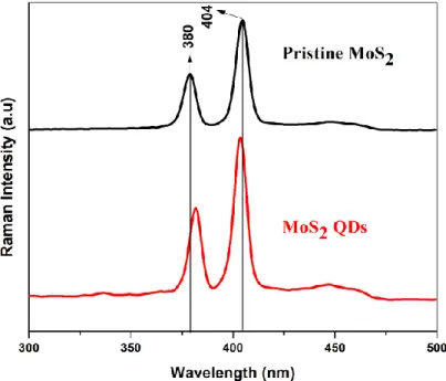
Fig. 2.3. Raman spectra of pristine MoS2 depicting two phonon modes E12g at 380 cm-1 and A1g
at 404 cm-1 respectively, while MoS2 QDs show red shift of E12g mode at 382 cm-1 and blue
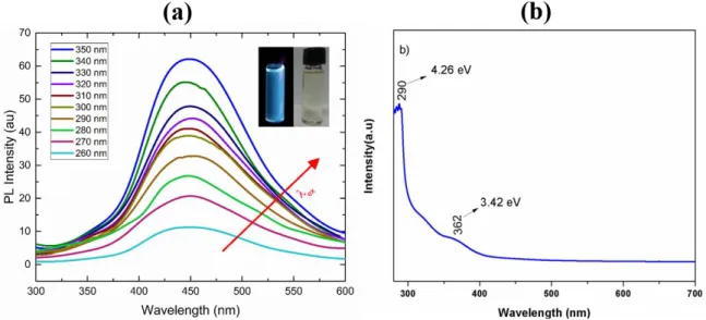
shift of A1g mode at 402 cm-1. ... 8 Fig. 2.4. (a) PL spectra of MoS2 QDs showing a distinct blue PL at 448 nm recorded at various
excitation wavelengths ranging from 260 to 350 nm. Inset: digital images of as prepared MoS2
QDs solution (right) and blue photo luminescent MoS2 QDs solution upon the UV illumination
at 365 nm. (b) UV-Vis absorption spectrum showing two bands at 290 nm and 362 nm. ... 9
Fig. 2.5. (a) FTIR spectra of MoS2 QDs showing a very weak absorption peak at 467 cm-1
which is attributed to the Mo−S stretching vibration mode of MoS2. (b) Energy dispersive
X-ray spectrum confirming the elemental composition of MoS2 QDs. ... 10
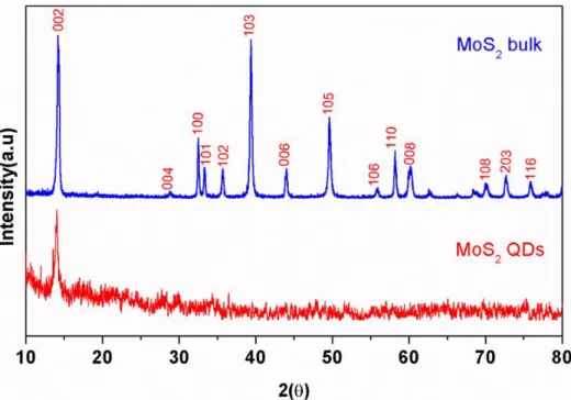
Fig. 2.6. XRD spectra of MoS2 bulk and MoS2 QDs, common peak for both phases of MoS2 is
observed at a value of 2θ of 14.2° which corresponds to (002) plane. ... 10
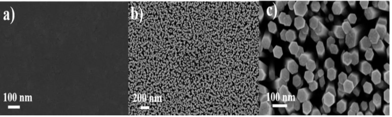
Fig. 2.7. (a) SEM image of ZnO seed layer (b) Highly dense and vertically aligned ZnO NWs
grown over the ZnO seed layer (c) SEM image on higher resolution showing truly hexagonal shape of ZnO NWs... 12
VIII
Fig. 2.8. Crystal structure of hexagonal wurtzite ZnO, and X-ray diffraction patterns of as
synthesized ZnO NWs grown on PET substrate showing high crystallinity. ... 13
Fig. 2.9. Morphology of the materials used in the humidity sensor (a) FESEM image of the as
exfoliated MoS2 flakes by aqueous exfoliation (b) FESEM images of MoS2 flakes thin film
deposited by EHDA showing the large lateral size flakes are uniformly dispersed on PET surface. ... 14
Fig. 2.10. Morphology of the as exfoliated hBN nanosheets by liquid exfoliation method and
its nanocomposite; (a) showing the FESEM image of the as exfoliated hBN nanoflakes. (b) AFM image of a single nanoflake after exfoliation showing the thickness up to 3 nm. ... 15
Fig. 2. 11. Raman spectra of as exfoliated hBN nanosheets showing E2g vibrational mode of
bulk and exfoliated phases at 1367 cm-1 and 1370 cm-1 respectively. ... 15
Fig. 2.12. (a,b) FESEM images showing cubic shape and uniform size of as synthesized
ZnSnO3 NCs via an aqueous solution method. ... 17
Fig. 2.13. (a) XRD patterns of ZnSn(OH)6 synthesized via an aqueous solution method at 80
˚C. (b) XRD patterns of ZnSnO3 nanocubes obtained after the calcination at 600 ˚C. ... 17
Fig. 2.14. (a) Raman spectra of ZnSn(OH)6 and ZnSnO3 nanocubes showing shifting of four
Raman modes to two new Raman modes after calcination at 600 ˚C for 3 h. FTIR spectra of
ZnSn(OH)6 and ZnSnO3 nanocubes exhibiting the conversion of ZnSn(OH)6 to ZnSnO3. .... 18
Fig. 2.15. (a,b) FESEM images of the as deposited ZnSnO3/PMMA nanocomposite thin film
through EHDA showing that ZnSnO2 NCs are fully covered by the blanket of polymer i.e. PMMA and film is uniform and smooth. ... 19
Fig. 2.16. (a) FTIR spectra of ZnSnO3/PMMA composite film on PET showing two peaks 538
and 617 cm-1 from ZnSnO3 and others are from PMMA. (b) Raman spectra of ZnSnO3/PMMA
composite film showing only one Raman active mode at 279 cm-1 from ZnSnO3 while others belong to PMMA. ... 20
IX
Fig. 2.17. (a) Transmittance and absorbance spectrums of ZnSnO3/PMMA deposited film on
PET by ESD. (b) I–V characteristic curve exhibiting the dielectric behavior of ZnSnO3/PMMA
composite film on PET with non-linear behavior and low magnitude of current. ... 21
Fig. 2.18. Structural formulas of inorganic perovskite oxide and organic polymer showing
interatomic chemical bonds and resulting hybrid nanocomposite solution. ... 22
Fig. 2. 19. Structural and optical characterization plots of as synthesized organic-inorganic
hybrid nanocomposite (a) XRD spectra (b) Raman spectra (c) UV-vis transmittance and absorbance spectra. ... 23
Fig. 2. 20. (a) Surface morphology of PVOH-ZnSnO3 hybrid nanocomposite thin film
exhibiting formation of granular polymeric network (b) Cross-section FESEM image illustrating the average thickness of as deposited thin film by EHDA. ... 24
Fig. 2.21. Schematic representation of the structures of hBN and PVOH on reactant side and
nanocomposite on product side. ... 25
Fig. 2.22. (a,b) FESEM images of the thin film of hBN/PVOH nanocomposite deposited by
EHDA. ... 26
Fig. 2.23. Optical characteristics; a) Raman spectra of as exfoliated hBN nanosheets showing
E2g vibrational mode of bulk and exfoliated phases at 1367 cm-1 and 1370 cm-1 respectively. b)
FTIR spectra of PVOH, hBN and their composite demonstrating the compositional analysis of aforementioned materials. c) UV/Vis analysis of as deposited hBN/PVOH nanocomposite thin film as deposited by EHDA showing low absorbance and high transmittance. ... 26
Fig. 2. 24. (a,b) ZnSnO3 NCs are interspersed onto ZnO NWs and some of the NCs are
incorporated into the pores of NWs. ... 28
Fig. 2.25. XRD spectra of ZnO NWS/ZnSnO3 nanocomposite showing the characteristic peaks
of both materials confirming their hexagonal wurtzite and rhombohedral structures respectively. ... 28
X
Fig. 3.1. Optical images of a) RPC printing head b) patterned circular top electrodes by RPC
head with three different sizes 42 µm, 70 µm and 100 µm respectively. ... 31
Fig. 3.2. Characteristic bipolar resistive switching curves of as prepared non-volatile flexible
memory devices based on hybrid hBN/PVOH nanocomposite a) Electroforming I-V curve to obtain repeatable results by forming a conductive path for further experiments b) I-V characteristic curve of 42 µm device c) I-V characteristic curve of 70 µm device d) I-V characteristic curve of 100 µm device. ... 32
Fig. 3.3. I-V characteristic curves of three different device sizes illustrating excellent endurance
and repeatability of bipolar resistive switching a-c) Illustration of high electrical endurance with 42 µm, 70 µm and 100 µm device size for 1000 biasing cycles. These curves are showing that the fabricated device has excellent repeatability validating the high dependability on fabrication technique d-f) I-V curves of each of the three fabricated memory cells with similar top electrode diameter of 42 µm, 70 µm and 100 µm respectively illustrating remarkable repeatability of fabricated devices. ... 33
Fig. 3.4. Cumulative Probability plots of threshold voltages and bistable resistive states a)
VSET and VRESET b) LRS and HRS of all the three device sizes. All these readings have been taken at a read voltage of 0.26 V c) Inverse relation of off/on ratio with applied external biasing voltage. ... 34
Fig. 3.5. Double logarithmic curves of all the three fabricated devices with different sizes
illustrating that all of them follow the same conduction mechanism of TSCLC based on their slope values. ... 35
Fig. 3.6. Illustration of formation and rupture of metallic filament from top electrode to bottom
electrode under the influence of strong electric field i) Off process in which atoms of Ag electrode oxidize and become Ag+ cations by losing electrons ii) SET process in which the trapped electrons begin to neutralize the Ag+ cations thus resulting in the formation of metallic
XI
filament within the functional layer of hBN-PVOH iii) At this point the metallic filament is completely formed from top to bottom electrode bringing the device into ON state iv) The formed filament is ruptured by applying electric potential of opposite polarity resulting in HRS b) Change in HRS and LRS with varying device size c) Dependence of bistable resistive states on temperature. ... 37
Fig. 3.7. Mechanical Bending test of the hybrid nanocomposite of hBN-PVOH to examine its
possible application in flexible electronic devices a) Maximum bending diameter up to which the performance of fabricated flexible memory device is showing highly repeatable results b) Mechanical bendability plot of the fabricated device illustrating highly stable results after 1500 bending cycles c) Layer by layer schematic diagram of ITO/hBN-PVOH/Ag resistive switch in bend state with labelling of each part and beside schematic the optical image of real device in bending state is shown. ... 38
Fig. 3.8. 3D view of various parts of Reverse Off-Set printing system displaying the step by
step patterning of bottom Ag electrodes on a flexible PET substrate a) Glass slide b) Ag nanoparticle ink spin coated on glass slide c) PDMS blanket roll lifting Ag ink from the glass slide d) Cliché design displaying the negative of desired bottom electrode patterns engraved on its surface e) Illustration of OFF Process in which PDMS blanket roll is shown to lift the electrode patterns from the cliché surface f) SET Process in which bottom Ag electrodes are transferred onto the desired PET substrate from the PDMS blanket roll. ... 40
Fig. 3.9. Electrical characterization of as prepared all printed, flexible and hybrid
organic-inorganic memory device based on PVOH-ZnSnO3 nanocomposite a) Typical log I-V
characteristic curve of a memristor illustrating bipolar resistive switching at a threshold voltage of ~ 1.5V b) Semi-logarithmic I-V curves displaying excellent repeatability for 1st, 250th, and 500th cycle c) Typical semi logarithmic I-V curves showing the bipolar resistive switching effect in all the 9 memory cells of a 9 × 1 matrix of as prepared memory device where M1-M9
XII
signify the labels of 9 memory cells respectively d) Endurance of memory device showing the value of both resistive states for each voltage sweep over 500 voltage cycles while maintaining the off/on ratio of > 102 measured at a reading voltage of 0.2 volt e) Retention of HRS and LRS measured for a longer period of time without any noticeable deviation with an off/on ratio of 1.65×10². All the resistance values were recorded at a reading voltage of 0.2 volts f) Optical
Image of as fabricated Ag/PVOH-ZnSnO3/Ag memory device on a flexible PET substrate in
bend condition. ... 42
Fig. 3.10. Double logarithmic I-V curve illustrating the slopes for LRS and HRS with unique
gradient values. This plot can be distributed into three separate regions as represented by the three different colors. In the green line region, Ohmic conduction takes place as gradient ≈ 1. The red line is the Child’s law region as the gradient value ≈ 3. The blue line shows the region of sharp current increase as gradient ≈ 32 where the device switches from HRS to LRS. ... 44
Fig. 3.11. Bendability measurements by using the in-house prepared bending machine
illustrating the remarkable flexible properties of as prepared resistive switching device a) Endurance plot clearly showing very less deviation in HRS and LRS with changing values of bending diameters in the range of 50 mm to 4 mm. The device behaved like an open circuit at a bending diameter of 4 mm. b) Typical semi-logarithmic I-V curve at three deferent values of bending diameters c) Endurance curve showing HRS and LRS values for 1500 bending cycles at a fixed diameter value of 15 mm d) Typical semi-logarithmic I-V curves before bending and after bending showing excellent repeatability of bipolar resistive switching. ... 48
Fig. 3.12. Originally printed cliché design consist of ten memory cells on PET (center), with
optical microscopic images of a single memory cell having width of 50 µm (left) and two consecutive memory cells (right). ... 50
XIII
Fig. 3.13. Schematic diagram of the as grown ZnO NWs on flexible substrate and their
heterostructure composite with ZnSnO3 NCs, after EHDA spray NCs were supposed to be
randomly oriented onto ZnO NWS while some of them infiltrated into their pores. ... 51
Fig.3. 14. Optical image of the real memory device showing the top electrode on active layers
patterned by EHD patterning (Center), optical microscopic images of the top electrode (right) and top electrode crossing above the bottom electrodes (left). ... 52
Fig. 3.15. Electrical characterization of as fabricated memory device (a) Electroforming step
before applying double voltage sweep (b) Characteristic bipolar I-V curve (c) Trend of switching ratio with increasing value of read voltage (d) Cumulative probability illustrating the distribution of bistable resistive states (e) Cumulative probability plot illustrating the distribution of Vth (Vset and Vreset)... 53
Fig. 3.16. (a) Illustration of high stability against several voltage cycles by displaying I-V
curves for 1st, 500th and 1000th cycle (b) Endurance of bistable resistive states for 1000 operating cycles (c) Retention I-V curves of as fabricated memory device for 1h, 2h and 3h respectively (d) High stability of bistable resistive states for a long retention time. ... 54
Fig. 3.17. Step by step fabrication process diagram; first IDTs were fabricated by using reverse
offset printing system, second thin film of MoS2 nanoflakes was fabricated through EHDA and
in last PEDO:PSS thin film was deposited by SAW-EHDA. ... 58
Fig. 3.18. Characterization setup used for the measurement of sensors’ electrical response
against relative humidity change ... 59
Fig. 3.19. Impedance response of sensors with active layers of (a) MoS2, (b) PEDOT:PSS, and
(c) Series combination of the two showing decrease in impedance with increasing relative humidity. ... 59
Fig. 3.20. Sensing mechanism of the sensors with active layers of (a) MoS2, (b) PEDOT:PSS,
XIV
Fig. 3.21. Frequency response of sensors with active layers of (a) MoS2, (b) PEDOT:PSS, and
(c) Series combination of the two showing drop in frequency output with increase in relative humidity. ... 63
Fig. 3.22. Frequency conversion circuit to translate the output of the sensors in to frequency (a)
circuit diagram of the designed oscillator and (b) actual photograph of the fabricated circuit. ... 64
Fig. 3.23. Response and recovery time curves of the sensors with active layers of (a) MoS2, (b)
XV
List of Tables
Table 3.1. Comparison of PVOH-ZnSnO3 nanocomposite based memristive device with
already reported ZnSnO3 memory device as reported in our previous work. It is evident from
the mentioned results that PVOH plays a vital role in improving the resistive switching characteristics of ZnSnO3 based memory device. ... 43 Table 3.2. Comparison of PVOH-ZnSnO3 nanocomposite resistive switching characteristics
with already reported other nanocomposite of PVOH polymer. ... 44
XVI
Abstract
There has been growing interest in the field of nanotechnology during the last two decades and nanostructured materials have the enormous contribution in this development. After the progress in synthesis of nanostructured materials, their functional characteristics were investigated and thus peculiar optical, chemical, electrical, mechanical and magnetic properties have been exploited. These nanostructured materials can be tailored to obtain desired characteristics by making their nanocomposites with various organic polymers or inorganic nanoparticles and their usage as thin films and coatings can further explore their applications in several fields.
This thesis reports a complete study based on synthesis, characterization, ink preparation, thin film fabrication and applications of functional nanostructured and nanocomposite materials. In this study, various low dimensional functional nanostructured materials have been
synthesized and developed including zero dimensional (0D) molybdenum sulfide (MoS2)
quantum dots (QDs), one dimensional (1D) zinc oxide (ZnO) nanowires (NWs), two
dimensional (2D) MoS2, and hexagonal boron nitride (hBN) nanosheets; and three dimensional
(3D) zinc stannate (ZnSnO3) nanocubes (NCs). Moreover, the nanocomposites of as
synthesized low dimensional nanostructured materials have also been reported that include
nanocomposite of ZnSnO3/PMMA, ZnSnO3/PVOH, hBN/PVOH, ZnO/ZnSnO3, and MoS2
-PEDOT:PSS. Applications of these nanostructures and nanocomposite materials have been presented by fabricating non-volatile resistive switching and humidity sensing devices using printing techniques like EHDA, reverse offset, SAW-EHDA, RPC, and EHD patterning. The morphological, structural, chemical, and optical characteristics of nanostructured and nanocomposite materials were analysed by using different characterization techniques like HR-TEM, FE-SEM, AFM, XRD, Raman, FTIR, EDX and UV/VIS spectroscopy. Furthermore, the
XVII
electrical and mechanical results have also been reported to show the performance and mechanical robustness of the fabricated devices.
1
Chapter -1. Introduction
1.1 Functional Nanostructured materialsNanostructured materials are the materials having at least one dimension lies between 1-100 nm in their structure. These may have various electronic nature based upon their electronic structure including conducting, semiconducting or dielectric so they may be termed as functional nanostructured materials. The synthesis of nanostructured materials is immensely significant research in the field of nanotechnology and captivating a large number of researchers. Their characterization and thin film fabrication for various devices has exploited numerous potential applications such as light emitting devices, memory devices, thin film transistors, photovoltaic devices, humidity sensors and bio-sensors.
1.2 Low-dimensional nanomaterials
Beside the composition and arrangement of atoms in materials, dimensionality plays a vital role in determining their fundamental characteristics. On the basis of dimension, nanostructured materials are categorized as 0D, 1D, 2D and 3D materials.
1.2.1 Zero-dimensional materials: Quantum dots
During the last two decades, a great deal of attention has been focused on quantum dots (zero-dimensional) which are few nanometre-scale (1-10 nm in diameter) [1] crystals of semiconducting materials. They have entirely different electronic, spectroscopic, and photophysical properties from their bulk because of quantum confinement and edge effects. Quantum dots (QDs) are being intensively investigated for applications such as light-emitting diodes, solid-state lighting, lasers, and solar cells. One useful feature of quantum dots is that the colors of light they absorb and emit can be tuned simply by varying their size [2], and this is because dots of the same material but different sizes have different band gaps, which absorb and emit different frequencies. Each semiconductor has a characteristic band gap, but when the diameter of a piece of the material is shorter than the quantum-mechanical wave function of its
2
electrons, the "squeezed" electron wave function makes the band gap wider. It means the smaller the quantum dot, the wider the band gap.
1.2.2 One-dimensional materials: Nanowires
One-dimensional nanomaterials may include whiskers, fibers or fibrils, Nanorods and nanowires but we have focused our studies on nanowires. They can be grown on various substrates from rigid to flexible. They exist in many forms including metals, semiconductors, insulators and organic compounds and are being studied for use in electronics, energy conversion, optics and chemical sensing, among other fields. The structure of nanowires is so simple that there is no room for defects, and electrons pass through unimpeded. The electrons and photons within these nanowires experience quantum confinement effects. The diameter of as grown nanowires is of few nanometers but their length can be extended for hundreds of micrometers and because of this, they have high ratio of surface are to volume. This unique characteristic makes them very good detectors, because all that surface area can be treated to bind with specific chemical or biological molecules. The electrical signal generated by that
binding can then easily be transmitted along the wire.
1.2.3 Two-dimensional materials: nanosheets or flakes
Two-dimensional materials or layered materials had become very popular after the discovery of graphene and since then the 2D materials are being explored in terms of their exfoliation methods, their electronic properties and their applications. They are consist of two-dimensional platelets weakly stacked to form three-dimensional structures [3]. They have strong in-plane chemical (covalent) bonds within each layer but weak out-of-plane van der Waals bonds. To get the maximum advantage of 2D materials, they must be exfoliated or delaminated to mono or few layers and over the past decade, a number of methods have been introduced that include
ultra-sonication [4–6], mechanical cleavage [7–10], Li-intercalation [11,12], and Sodium naphthalenide [13]. The mono or few-layer exfoliated MoS2 has intriguing applications such as super capacitor [14],
3
electro catalyst for hydrogen evolution reaction (HER) [15,16], sensor [17], field effect transistor [18,19], and solar cells [20,21].
1.2.4 Three-dimensional Materials: nanocubes
Nanocubes are the cube shaped nanoparticles having size of few nanometers. The distinctive morphology and homogeneity of the nanocubes makes them ideal for use in: surface-enhanced Raman scattering (SERS), metamaterials, plasmonic catalysis and photovoltaics and other
energy harvesting devices. ZnSnO3 NCS have been used more oftenly for different application
then other nanocubes such as gas sensor, humidity sensor, nanogenerator, memristor and photocatalysis [22–26].
1.3 Nanocomposites
Nanocomposites are combination of two materials usually organic-inorganic based materials that incorporate nanosized particles into a matrix of standard material. Polymer based or organic-inorganic nanocomposite materials are promising systems for a variety of applications due to their extraordinary properties, which arise from the synergism between the properties of the components. There are several routes to these materials, but probably the most prominent one is the incorporation of inorganic nanostructures in organic polymers. These materials have gained much interest due to the remarkable change in properties such as mechanical, [27]
thermal, [28]electrical, [29]and magnetic [30]compared to pure organic polymers. They have
the combined distinct characteristics of organic and inorganic materials and both type of materials have certain advantages when used in electronic devices. Organic materials are manifold in their properties such as easy and low temperature processing, economical fabrication, high flexibility, and large area fabrication. Inorganic materials have excellent thermal and mechanical stability, high carrier mobilities, and wide range of optical, electrical, magnetic and dielectric properties.
4
Chapter 2- Synthesis of Nanomaterials and Nanocomposites
2.1. Synthesis of MoS2 QDs
MoS2 QDs were prepared by wet grinding followed by mechanical shaking, bath sonication,
ultrasound probe sonication and centrifugation. MoS2 powder was ground in NMP in a mortar
for 6 hours; after grinding, the gel like mixture was dried for 1 hour at 100 °C. The dried MoS2
powder was then dissolved in equal volumes of NMP and DCB and kept on magnetic stirrer
for 30 min followed by mechanical shaking for 4 hours at 300 rpm. Bath sonication of MoS2
solution was carried out for 4 hours followed by ultrasound probe sonication for 1 hour. After performing these processes, the solution was kept undisturbed for overnight and top 2/3 portion
of the MoS2 solution was carefully taken out for centrifugation. The centrifugation was carried
out for 30 min at 8000 rpm and supernatant was obtained by decantation. Thus the solution of
MoS2 QDs was obtained and used for further characterizations. The solution was finally dried
in order to calculate the concentration (yield) of as synthesized MoS2 QDs. The schematic
diagram to synthesize MoS2 QDs is also depicted in Fig. 2.1.
MoS2 QDs were prepared by wet grinding in NMP assisted bath and probe sonication in NMP
and DCB. The color of the bulk MoS2 solution is dark grey but after performing all the
processes it becomes faint yellow as shown in Fig. 2.1.
In fact, the direct dispersion of TMDs in solvents causes the low concentration of mono or few layers [31,5]. Hence, grinding makes a useful effect in exfoliation of layered materials because it generates shear forces to detach the layers of 2D materials. Many organic solvents like N-cyclohexyl-2-pyrrolidone, tetrahydrofuran, ethylene glycol, dimethylformamide, dimethyl sulfoxide, chlorobenzene, pyridine and many others have been used for liquid exfoliation of layered materials but both NMP and DCB are suitable solvents for exfoliation and stable
5
dispersion of 2D materials [32]. For the better dispersion of TMDs, solvents having surface tension values in range of 40 mN/m to 50 mN/m or surface energy value close to 70 mN/m are
Fig. 2.1. Schematic diagram for the synthesis of MoS2 QDs consist on wet grinding in NMP followed by
mechanical shaking for 4 h, bath sonication for 4 h, probe sonication for 1 h and centrifugation at 8000 rpm for 30 min.
preferred [5,33]. When surface energy values of organic solvents and TMDs match with each
other, a good dispersion is observed [31]. For the synthesis of MoS2 QDs, ultrafine MoS2
powder was used because it has smaller flakes, and creates dispersion with smaller particle size whereas micropowder requires more sonication and will result flakes with larger lateral dimensions. In this experiment, we used NMP first for wet grinding and further for dispersion
because it acts as a stabilizing agent to avoid the restacking of the MoS2 nanosheets or
nanoparticles [34] while DCB also improves exfoliation, stable dispersion and high
concentration of MoS2 nanosheets [35]. Ultrasound sonication in mixed solvents is an attractive
route to exfoliate TMDs [5,36,37]. We also used this strategy to synthesize MoS2 QDs using
bath and probe sonication in NMP and DCB and it was found to be an efficient method because
6
sonication, the increase in temperature and pressure of the solution results the generation of hydrodynamic forces which cleave larger particles into smaller particles [38].
The size and morphology of the as synthesized MoS2 QDs was measured by HR-TEM. In Fig. 2.2 (a) it can be clearly observed that most of the MoS2 QDs synthesized by this method are very small, uniform in size and their concentration is appreciable as well. The distribution of quantum dots is shown by plotting histogram as shown in Fig. 2.2 (b), (the size is statically calculated from more than 200 QDs in TEM image) all the QDs are ≤ 7.5 nm and majority lies
in the range of 2-5 nm which indicates the efficacy of our strategy to synthesize MoS2 QDs.
Typical selected area electron diffraction (SAED) pattern as shown in Fig. 2.2 (c) reveals the
six-fold symmetry hexagonal lattice and high crystallinity of MoS2. In Fig. 2.2 (d) magnified
TEM image shows the hexagonal lattice structure and high crystallinity of MoS2 QDs with
lattice spacing of 0.23 nm which corresponds to the (103) plane of MoS2 and similar to
hexagonal pattern of MoS2 mono or few layer.
Raman spectroscopy is a powerful non-destructive characterization tool in the study of layered materials in which the coupling between electronic structure and phonons is studied. Generally,
four phonon modes E22g, E1g, E12g and A1g are observed in bulk MoS2 but only two of them
E1
2g and A1g, are associated with the thickness of the MoS2 layer [39]. Generally, in the
exfoliated MoS2 monolayer, E12g mode is red-shifted and A1g mode is blue-shifted [2,39,40].
In Fig. 2.3, two phonon modes of pristine MoS2, E12g at 380 cm-1 and A1g at 404 cm-1 were
observed, while these phonon modes were shifted at 382 cm-1 (red-shift) and 402 cm -1
(blue-shift) in MoS2 QDs. The results of this study are in well agreement with already reported
Raman analysis of exfoliated MoS2 monolayer [2,39,40]. The E12g mode is associated with
opposite vibration of two sulfur atoms with respect to molybdenum atom and A1g mode is
7
Fig. 2.2. (a) High resolution TEM image of MoS2 QDs showing good concentration and uniformity. (b) Histogram
showing the distribution of QDs, most of the QDs are in range of 2-5 nm. (C) SAED pattern which reveals the six-fold symmetry hexagonal lattice and high crystallinity of MoS2 QDs. (d) Magnified TEM image showing the
lattice spacing 0.23 nm corresponds to (103) plane.
The Raman frequencies of these two phonon modes vary monotonously with the layer numbers
of MoS2 and are reliable features to identify the number of layers with much higher accuracy
than the intensities and width of the peaks. The gap between the frequencies of these two phonon modes depends upon the method of exfoliation, a close gap shows that monolayer
structure is more prominent. Frequency of the E1
2g mode decreases and A1g mode increases,
when number of layers of MoS2 are increased [41,42].
The optical properties of as synthesized MoS2 QDs were explored by PL spectroscopy. PL
spectroscopy is a contactless, non-destructive technique of probing electronic structure of
materials. The absence of luminescence in bulk MoS2 and strong emerging photoluminescence
8
the synthesis of strong photoluminescence MoS2 QDs, the exfoliation of bulk MoS2 to
monolayer is a pre-requisite and important step.
Fig. 2.3. Raman spectra of pristine MoS2 depicting two phonon modes E12g at 380 cm-1 and A1g at 404 cm-1
respectively, while MoS2 QDs show red shift of E12g mode at 382 cm-1 and blue shift of A1g mode at 402 cm-1.
When the size of the exfoliated mono layer MoS2 is less than 100 nm, it leads to the
confinement and edge effects which causes the photoluminescence emission [38]. Due to the
transition from indirect to direct band gap MoS2 nanostructures show unique
photoluminescence properties. Fig. 2.4 (a) exhibits that as synthesized MoS2 QDs emitted a
distinct blue PL at 448 nm regardless of the excitation wavelength when they were excited at various excitation wavelengths ranging from 260 nm to 350 nm which shows high homogeneity.
This range also confirms that size of MoS2 QDs synthesized by this approach is very small
because luminescence properties of QDs are dependent upon their size [38]. The as synthesized
MoS2 QDs showed a distinct blue luminescence (Inset of Fig. 2.4 a) when illuminated under
365 nm UV illumination.
Optical properties were further investigated by UV-Vis spectroscopy. Two absorption band were observed at 290 nm (4.26 eV) and at 362 nm (3.42 eV) respectively as shown in Fig. 2.4
9
are 3.5 nm in size (as shown in Fig. 2.2 b) and are in well agreement with previously reported
absorption spectra of MoS2 nanoclusters [43].
Fig. 2.4. (a) PL spectra of MoS2 QDs showing a distinct blue PL at 448 nm recorded at various excitation
wavelengths ranging from 260 to 350 nm. Inset: digital images of as prepared MoS2 QDs solution (right) and blue
photo luminescent MoS2 QDs solution upon the UV illumination at 365 nm. (b) UV-Vis absorption spectrum
showing two bands at 290 nm and 362 nm.
Chemical and elemental composition were analysed by FTIR spectroscopy and energy dispersive X-ray (EDX) spectroscopy shown in Fig. 2.5 (a) and 5 (b) respectively. In Fig. 2.5
(a), a very weak absorption peak can be observed at 467 cm-1 which is attributed to the Mo−S
stretching vibration mode of MoS2. FTIR spectra of the exfoliated MoS2 remain same as of
bulk MoS2 [42]. EDX analysis was also applied to determine the elemental composition of as
synthesized MoS2 QDs which confirms the presence of Mo and S as shown in Fig. 2.5(b). The
peaks indicate that sample contains Mo, S and Cu. The highest peak recorded belongs to Cu grid support for measurement. The atomic ratio of S to Mo was calculated about 2.12 which is
quite close to the theoretical value of MoS2. These values confirm that the products were
stoichiometric MoS2.
The crystal structure of as synthesized MoS2 QDs was investigated using XRD system. The
reflection peaks can be assigned to the family lattice planes of hexagonal MoS2 (JCPDS card
10
Fig. 2.5. (a) FTIR spectra of MoS2 QDs showing a very weak absorption peak at 467 cm-1 which is attributed to
the Mo−S stretching vibration mode of MoS2. (b) Energy dispersive X-ray spectrum confirming the elemental
composition of MoS2 QDs.
Three dominant peaks can be observed at 14.2° (002), 39.5° (103) and 49.8° (105) respectively
in pristine sample whereas only one weak peak is obtained in case of MoS2 QDs that is
attributed to (002) plane and occupies the similar position to pristine MoS2 which means no
other new phases are introduced into MoS2 QDs. So it can be concluded from XRD data that
pristine MoS2 and MoS2 QDs both are identified as 2H MoS2 with prominent peak at 14.2°
belonging to (002) plane.
Fig. 2.6. XRD spectra of MoS2 bulk and MoS2 QDs, common peak for both phases of MoS2 is observed at a value
11
2.2. Hydrothermal growth of ZnO nanowires
For vertically aligned, highly dense and uniform growth of ZnO NWs, the deposition of ZnO seed layer is considered prerequisite so first, for deposition of ZnO seed layer, 20 mM
Zn(CH3COO)2.2H2O solution was prepared by dissolving it in anhydrous ethanol. ZnO seed
layer was deposited on top of as fabricated bottom electrode patterns on PET by reverse offset. ZnO seed layer solution was spin coated in such a way that after depositing one layer, PET was annealed at 95 ˚C for 10 min and this process was repeated 5 times and finally annealed at 95 ˚C for 3 hours. The all process was repeated once again to get a distinct white layer to ensure the better growth of ZnO seed layer.
ZnO NWs were grown by hydrothermal synthesis using equimolar (40 mM) aqueous solutions
of Zn(NO3)2.6H2O and HMTA in deionized water. The PET substrate printed with bottom
electrodes and ZnO seed layer over it was immersed in the aqueous solution upside down in an autoclave and heated at 95 ˚C for 3 hours. Finally, after heating the PET substrate was taken out and washed with deionized water several times to remove surface contaminations and dried in an open air.
The growth of the ZnO nanowires may take place through the following chemical reactions:
(CH2)6N4 + 6H2O → 6HCHO + 4NH3 (1)
NH3 + H2O → NH4+ + OH ̶ (2)
Zn2+ + 2OH ̶ → Zn(OH)2 (3)
Zn(OH)2 → ZnO + H2O (4)
2.2.1 Material Characterization
Morphology of the deposited ZnO seed layer and as grown ZnO NWs on ZnO seed layer has been analyzed by FESEM images as shown in Fig. 2.7. ZnO NWs grown by hydrothermal
12
synthesis were found to be highly dense, aligned and vertically oriented with hexagonal crystal structure as shown in Fig. 2.7 (b) & (c). Their size was also observed very uniform, average
diameter was found to be 100 nm, average length (0.5 µm), and average density (1×2 109 cm
-2). In fact, the growth of such highly aligned and dense ZnO NWs is related to the quality of
the ZnO seed layer; unsmoothed, defected ZnO seeding layer results in the non-vertical and random distribution of ZnO NWs. Fig. 2.7 (a) shows the FESEM image of the compact ZnO seed layer proving that the surface morphologies of these hydrothermally grown ZnO NWs strongly depend upon the ZnO seeding layer.
Fig. 2.7. (a) SEM image of ZnO seed layer (b) Highly dense and vertically aligned ZnO NWs grown over the ZnO
seed layer (c) SEM image on higher resolution showing truly hexagonal shape of ZnO NWs.
X-Ray diffraction patterns of ZnO nanowires, has been shown in Fig. 2.8. The patterns clearly reveal the diffraction peaks at 31.61, 34.49, 36.27, 56.32 and 62.63 corresponding to (100), (002), (101), (110) and (103) planes that can be indexed to hexagonal wurtzite crystal structure of ZnO NWs.[44] These diffraction peaks indicating the purity of ZnO NWs due to absence of other peaks related to impurities and are in well agreement with JCPDS card no. 36-1451 with cell constants of a = 3.25 Å and c = 5.19 Å . The dominant diffraction peak at 2θ = 34.49 corresponding to the (002) plane indicates high degree of anisotropic growth of ZnO NWs along c-axis perpendicular to the PET substrate and highly crystalline in nature.
13
Fig. 2.8. Crystal structure of hexagonal wurtzite ZnO, and X-ray diffraction patterns of as synthesized ZnO NWs grown on PET substrate showing high crystallinity.
2.3. Liquid based exfoliation of 2D materials
Liquid exfoliation of layered or 2D materials has certain advantages as it is solution processable, easy to make inks and composite and ease of fabrication of thin film on various substrate from rigid to flexible substrates.
2.3.1 Exfoliation of MoS2 and characterization
MoS2 nanoflakes ink was prepared by exfoliating the MoS2 multi flakes by aqueous exfoliation
method. MoS2 pristine powder was ground in ethanol for 1 hour in a mortar followed by heating
at 100 °C for 1 hour to evaporate the solvent. Furthermore, ground MoS2 was dispersed in
50/50 % solution of ethanol and deionized water for probe sonication for 1 hour as grinding
and sonication both are effective in exfoliation of MoS2 flakes. Finally, centrifugation at 4000
rpm was carried out for 30 min to remove the larger flakes and partially exfoliated crystallites. The supernatant was collected and placed on magnetic stirrer for overnight.
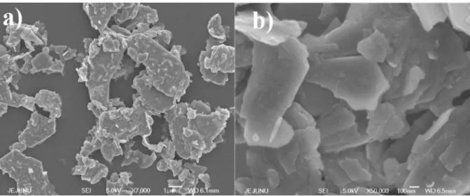
Morphology of the as exfoliated MoS2 flakes by aqueous exfoliation has been shown in Fig.
2.9 (a). It cab seen that MoS2 flakes of various size from several nanometer to few micrometer
14
2.9 (b) shows the morphology of as deposited thin film of MoS2 flakes through EHDA, a
uniform film of MoS2 flakes of various size and it can be seen that MoS2 exfoliated flakes are
dispersed uniformly on PET surface.
Fig. 2.9. Morphology of the materials used in the humidity sensor (a) FESEM image of the as exfoliated MoS2
flakes by aqueous exfoliation (b) FESEM images of MoS2 flakes thin film deposited by EHDA showing the large
lateral size flakes are uniformly dispersed on PET surface.
2.3.2 Exfoliation of h-BN and characterization
Exfoliation of bulk BN flakes was conducted on liquid based method to make a stable solution. First of all the wet grinding was carried out of pristine BN in a mortar by adding few drops of IPA for 2 hours and after drying the wet mixture it was dispersed in IPA. This dispersion was sonicated in an ultrasonic bath sonicator for 1 hour followed by ultrasonic probe sonication for 1 hour at high frequency. Further to separate the bulk or large unexfoliated flakes, the as prepared dispersion was centrifuged at 4000 rpm for 30 min and top 3/4 supernatant was taken out in a vial.
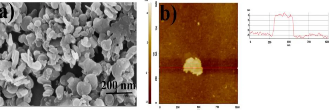
The surface morphology, topography and orientation of the as exfoliated hBN nanosheets
was investigated using FESEM. Fig.2.10 (a) shows the microstructure and lateral size of as
exfoliated hBN nanoflakes. The AFM image has been shown in Fig. 2.10 (b) which shows the thickness of a single exfoliated hBN nanoflake up to 3 nm along the red line and its
15
corresponding height profile. This AFM data exhibits that the liquid based exfoliation has also potential for producing thin nanosheets of 2D materials as these very thin nanosheets are useful for resistive switching effect.
Fig. 2.10. Morphology of the as exfoliated hBN nanosheets by liquid exfoliation method and its nanocomposite;
(a) showing the FESEM image of the as exfoliated hBN nanoflakes. (b) AFM image of a single nanoflake after exfoliation showing the thickness up to 3 nm.
Raman spectroscopy was used to investigate the exfoliation of BN 2D flakes. Fig.2.11 shows
the Raman spectra of both bulk and exfoliated BN flakes. The E2g vibrational mode is observed
in unexfoliated or pristine and exfoliated hBN which is the characteristic of hBN structure. In
pristine hBN the E2g mode is observed at 1367 cm -1 while in exfoliated hBN it is observed at
1370 cm-1 [45,46]. So, there is a blue shift of the E2g vibrational mode up to 3 cm-1 in exfoliated
hBN which is quite comparable with the earlier reported results[46,47].
Fig. 2. 11. Raman spectra of as exfoliated hBN nanosheets showing E2g vibrational mode of bulk and exfoliated
16
2.4. Synthesis of ZnSnO3 Nanocubes
Synthesis of crystalline ZnSnO3 nanocubes was carried out via aqueous solution method; 100
mmoles of ZnSO4.7H2O were added in 100 ml of deionized (DI) water and stirred at room
temperature until the complete dissolution of ZnSO4.7H2O. Then 100 mmol of Na2SnO3.3H2O
were added into the preliminary solution and was kept on magnetic stirrer at 80 ˚C for 5 h. A
white suspension of an intermediate product ZnSn(OH)6 was formed which precipitates were
collected from the solution by vacuum filtration and were washed with DI water several times to remove residual products and were then dried in air at 100 ˚C for 1 h. Afterwards, the as
synthesized ZnSn(OH)6 powder was calcinated at 600 ˚C for 3 h. Finally, we got the ZnSnO3
nanocubes by the following possible reaction: Zn2++2OH- → Zn(OH)
2 (5)
Zn(OH)2+ SnO32- +3H2O → ZnSn(OH)6 + 2OH- (6)
ZnSn(OH)6 → ZnSnO3+ 3H2O (7)
2.4.1 Material Characterization
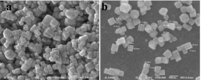
ZnSnO3 nanocubes was investigated by FE-SEM as shown in Fig. 2.12 (a,b).It reveals clearly
the cubic shape of ZnSnO3 nanostructures having an average size of approximately 70 nm and
also showing the large-scale, uniform cubic crystallites yielded with this approach.
An intermediate product zinc hydroxystannate (ZnSn(OH)6) is formed before the yield of
ZnSnO3 nanocubes. They were obtained by carrying out the chemical reaction between
ZnSO4.7H2O and Na2SnO3.3H2O at 80˚C for 5 h which on further calcination at 600 ˚C for 3
hours converted to the desired product, i.e. ZnSnO3 nanocubes. Fig. 2.13 (a) shows the XRD
patterns of the ZnSn(OH)6 material obtained at 80 ˚C . All the diffraction peaks are in good
17
Fig. 2.12. (a,b) FESEM images showing cubic shape and uniform size of as synthesized ZnSnO3 NCs via an aqueous solution method.
The crystalline structure of ZnSnO3 nanocubes is confirmed by XRD as shown in Fig. 2.13 (b),
all of the indicating diffraction peaks can be indexed to the JCPDS card No. 28-1486. The XRD
spectrum also indicates that ZnSnO3 nanocubes have pure crystalline structure and there are no
impure phases in it. So, overall it shows a large surface area, high crystallinity, smaller particle size and uniform morphology.
Fig. 2.13. (a) XRD patterns of ZnSn(OH)6 synthesized via an aqueous solution method at 80 ˚C. (b) XRD patterns
of ZnSnO3 nanocubes obtained after the calcination at 600 ˚C.
To investigate the composition of ZnSn(OH)6 and ZnSnO3, Raman and FTIR spectra were
18
[49,26]. Fig. 2.14 (a) represents the Raman spectra of both materials ZnSn(OH)6 and ZnSnO3
in which four Raman modes can be seen at 299, 372, 436 and 608 cm-1 for ZnSn(OH)
6 arising
from the breathing vibrations of the long M–OH bonds and M–OH–M (bridging OH group)
bending modes. After heating the ZnSn(OH)6 at 600 ˚C for 3 hours the above mentioned four
Raman modes were slightly shifted to two new Raman modes at 538 and 671 cm-1. The broad
peak at 671 cm-1 corresponds to the distinctive Raman shift of ZnSnO
3 and is imputed to
stretching vibrations of short M–O bonds in the MO6 octahedron that protrude into the structure
spaces. The peak at 538 cm-1 is assorted with internal vibrations of the oxygen tetrahedron.
Fig. 2.14. (a) Raman spectra of ZnSn(OH)6 and ZnSnO3 nanocubes showing shifting of four Raman modes to two
new Raman modes after calcination at 600 ˚C for 3 h. FTIR spectra of ZnSn(OH)6 and ZnSnO3 nanocubes
exhibiting the conversion of ZnSn(OH)6 to ZnSnO3.
The FTIR spectra of both ZnSn(OH)6 and ZnSnO3 are shown in Fig. 2.14 (b). The bands at
~3213cm-1 is ascribed to the bending and stretching vibration modes of hydroxyl (–OH) group
in the structure of ZnSn(OH)6. The bands at 779, 848, 1176, and ~2309 cm-1 may be attributed
to vibration of M–O or M–OH–M groups for ZnSn(OH)6 while the bands at 533, 572, and
1113 cm-1 are assigned to vibrations of M–O or M–O–M groups for ZnSnO
3. It was observed
from the spectral data that, after calcination the peaks of the (–OH) group almost disappeared while the peaks attributed to the M–O bond became prominent which testified the conversion
19
2.5. Nanocomposite of ZnSnO3/PMMA
The ZnSnO3 nanocubes were synthesized by aqueous solution method as described in detail in
section 2.4. The PMMA solution was prepared by dissolving 0.10 g of PMMA in 10 ml of toluene and kept on bath sonicator for 5 min and then kept for stirring at 40 ˚C for 24 hours.
The as synthesized ZnSO3 nanocubes were then dispersed in PMMA solution. For the better
dispersion of ZnSnO3 nanocubes into PMMA solution, it was sonicated for 30 min and a
non-ionic surfactant, i.e. 0.01% Triton X-100 (Sigma Aldrich) was also added for the same purpose and kept on stirrer at room temperature for overnight to check the stability of the synthesized ink. To improve the quality of the film and to meet the conductivity requirements for electrospray deposition, the co-solvent approach was adopted [50,51] and dimethyl sulfoxide
(DMSO) was added to ZnSnO3/PMMA ink in a ratio of 1:5.
2.5.1 Characterization of ZnSnO3/PMMA nanocomposite thin film
FE-SEM image of ZnSnO3/PMMA thin film has been presented in Fig. 2.15 (a,b) showing that
the film surface is mainly covered by the PMMA and ZnSnO3 nanocubes are buried PMMA.
Moreover, the film is highly uniform and compact and has the potential to be used in various electronic devices.
Fig. 2.15. (a,b) FESEM images of the as deposited ZnSnO3/PMMA nanocomposite thin film through EHDA showing that ZnSnO2 NCs are fully covered by the blanket of polymer i.e. PMMA and film is uniform and smooth.
20
The FTIR spectra of ZnSnO3-PMMA nanocomposite thin film is shown in Fig. 2.16 (a) in
which both ZnSnO3 and PMMA peaks are present, but most of the peaks belong to PMMA and
agree well with the values of the FTIR spectra of PMMA reported in the literature [52,53]. The
peaks at 538 and 617 cm-1 are attributed to the vibrations of M–O or M–O–M groups for
ZnSnO3. The peaks at 696 and 750 cm-1 are assigned to out of plane OH bending. The band at
987 cm-1 is the characteristic absorption of PMMA, together with the band at 1067 cm-1. The
peak observed at 1151cm-1 is assigned to C–O stretching, whereas the peak observed at 1452
cm-1 is assigned to O–CH
3 bending and at 1733 cm-1 is attributed to C=O stretching which
shows the presence of the acrylate carboxyl group. The two peaks at 3446 and 1541 cm-1 can
be attributed to the –OH group stretching and bending vibrations of physisorbed moisture [54].
Fig. 2.16. (a) FTIR spectra of ZnSnO3/PMMA composite film on PET showing two peaks 538 and 617 cm-1 from
ZnSnO3 and others are from PMMA. (b) Raman spectra of ZnSnO3/PMMA composite film showing only one
Raman active mode at 279 cm-1 from ZnSnO3 while others belong to PMMA.
Raman scattering of ZnSnO3/PMMA composite film has been shown in Fig. 2.16 (b) that
exhibits only one Raman active mode at 279 cm-1 from ZnSnO3 while other Raman modes noticed in the spectra are from PMMA [55,56].
Transmittance and absorbance of as deposited ZnSnO3/PMMA film on PET was carried out by
21
transmittance and low absorbance of the deposited film of ZnSnO3/PMMA on PET. It shows
an average transmittance of 92%, which indicates that it can be very useful in transparent electronics.
Fig. 2.17. (a) Transmittance and absorbance spectrums of ZnSnO3/PMMA deposited film on PET by ESD. (b) I–
V characteristic curve exhibiting the dielectric behavior of ZnSnO3/PMMA composite film on PET with
non-linear behavior and low magnitude of current.
Electrical properties of ZnSnO3/PMMA film were measured by semiconductor device analyzer
by placing the probes of device on silver contacts deposited on the ZnSnO3/PMMA film so that
they may not damage the film. The I-V plot for an approximately 110 nm thick ZnSnO3/PMMA
film is shown in Fig. 2.17 (b). The I-V plot shows very low currents and high resistance at low applied potentials. The resistivity was measured from the slopes of the linear I-V plot and using
the sheet resistivity formula for thin films:
𝜌 = 𝜋𝑡 ln 2(
𝑉
𝐼) Where ‘t’ is the thickness of the film (110 nm), while ‘V’ is voltage and ‘I’ is the current from the I-V plot. The calculated resistivity came out to be ≈ 34.88 × 10³ Ω.m. As a passive
component we can include the use of this material as dielectric for a wide range of electronic devices.
22
2.6. Nanocomposite of ZnSnO3/Polyvinyl alcohol (PVOH)
The ZnSnO3 nanocubes were synthesized by aqueous solution method as described in detail
section 2.4. The nanocomposite ink of PVOH-ZnSnO3 was prepared in NMP solvent, first 10
wt.% PVOH was dissolved in NMP followed by bath sonication for 10 min in an ultrasonic bath sonicator. The resulting solution was stirred on a magnetic stirrer at 70 ˚C until all the
PVOH polymer was completely dissolved in NMP. ZnSnO3 nanocubes (1 wt.%) were
dispersed in the PVOH solution and sonicated in an ultrasonic probe sonicator to enhance homogeneity. The final solution was stirred on a magnetic stirrer to check the stability of the ink for overnight at room temperature. The formation of the granular polymer network by
mixing the inorganic perovskite ZnSnO3 nanocubes and PVOH has been illustrated in Fig. 2.18.
Fig. 2.18. Structural formulas of inorganic perovskite oxide and organic polymer showing interatomic chemical bonds and resulting hybrid nanocomposite solution.
2.6.1 Characterization of thin film of ZnSnO3/PVOH
X-ray diffraction (XRD) is a powerful technique to understand the various characteristics of thin films including determination of crystalline structure and phase analysis. The XRD pattern
of PVOH-ZnSnO3 composite thin film has been shown in Fig. 2.19 (a). The large and broad
diffraction peak located at 2θ = 19.04˚ corresponds to (101) plane and exhibited the semi-crystalline nature of PVOH [57]. The small hump like pattern located at 2θ = 39.24˚ depicted
the presence of ZnSnO3 nanocubes. As the concentration of ZnSnO3 is low compared to PVOH
23
that the prepared thin film of PVOH-ZnSnO3 nanocomposite consists of only two phases i.e.
PVOH and ZnSnO3 and ruled out the presence of other phases or impurities.
Fig. 2. 19. Structural and optical characterization plots of as synthesized organic-inorganic hybrid nanocomposite
(a) XRD spectra (b) Raman spectra (c) UV-vis transmittance and absorbance spectra.
Optical characterization of Fourier Transform Infrared (FTIR) spectroscopy was carried out for
determining the chemical composition and interatomic bonding of PVOH-ZnSnO3 hybrid thin
film in the IR region of the electromagnetic spectrum as shown Fig. 2.19 (b). The broad peak
at 3422 cm-1 is assigned to the hydrogen-bonded O˗H stretching due to the absorption of
moisture. The peak at 2921 cm-1 is attributed to the asymmetric stretching vibration of CH2
group. The two bands at 1739 cm-1 and 1653 cm-1 correspond to the C=O stretching vibrations
in the acetate group and C=C stretching mode of PVOH respectively. The band appeared at
1455 cm-1 is attributed to the bending deformation of CH2 vibrations. The out-of-plane O˗H
bending vibration and in-plane O˗H bending vibration are observed at 1375 cm-1 and 668 cm-1
respectively. The other two bands observed at 1266 cm-1 and 1094 cm-1 correspond to the O˗C
stretching vibrations. Most of the peaks described in the FTIR spectra are related to the PVOH polymer and well matched with the earlier reported nanocomposite thin films of PVOH [57,58].
The single peak at 516 cm-1 is assigned to the presence of ZnSnO3 in this nanocomposite thin
film [59]. Thus FTIR spectra revealed the formation of PVOH and ZnSnO3 nanocomposite
with no other impurities and also proved the effective infiltration of ZnSnO3 nanocubes into
the polymer matrix of PVOH.
The UV-vis transmittance and absorbance spectra of PVOH-ZnSnO3 nanocomposite thin film
24
absorbance spectra are merged in Fig. 2.19 (c). The PVOH film is highly transparent (~ 90% transmittance across the visible light region) making it extremely useful in various optical
applications as reported by Wang et al [60]. In this work; by the addition of ZnSnO3 nanocubes
into the polymer matrix of PVOH for the formation of granular polymer network, the transparency has not affected much and found to be ~ 84%.
Fig. 2.20 (a) illustrates the surface morphology of the nanocomposite thin film as deposited by EHDA which exhibited the formation of granular polymeric network. Furthermore, SEM
images also revealed that ZnSnO3 nanocubes are homogeneously embedded into the polymer
matrix of PVOH resulting in the formation of granular polymer network. The thickness of thin film was measured by cross-sectional FESEM image as shown in Fig. 2.20 (b) and it appeared to be ≈ 238 nm.
Fig. 2. 20. (a)Surface morphology of PVOH-ZnSnO3 hybrid nanocomposite thin film exhibiting formation of
granular polymeric network (b) Cross-section FESEM image illustrating the average thickness of as deposited thin film by EHDA.
2.7. Nanocomposite of hBN/PVOH
Exfoliated of bulk hBN flakes has been described in detail in section 2.3.2. The polymer ink was prepared by dissolving PVOH powder in DI water at 80 ˚C and placed on magnetic stirrer until a transparent solution is formed on complete dissolution of powder. Both, the as prepared hBN solution in IPA and PVOH solution in DI water were homogenously mixed in equal volumes and stirred at high rpm by placing it on magnetic stirrer for overnight to check the
25
stability of the mixed solution. The schematic of the hBN/PVOH nanocomposite has been shown in Fig. 2.21 in which the structures of hBN and PVOH are exhibited on reactant side and crosslinked nanocomposite of exfoliated hBN nanosheets with polymer chain on the product side. Structure of PVOH shows that it is a branched polymer, significantly suitable for coating a 2D material to form a highly uniform thin film.
Fig. 2.21. Schematic representation of the structures of hBN and PVOH on reactant side and nanocomposite on
product side.
2.7.1 Characterization of thin film of hBN/PVOH nanocomposite
The surface morphology and topography of hBN/PVOH nanocomposite was investigated using FESEM. The morphology of the thin film of hBN/PVOH nanocomposite fabricated by EHDA has been shown in Fig. 2.22 (a,b), it can be observed that hBN nanoflakes are well mixed in the polymeric network of PVOH and wrapped up by the polymer. Both the images show the composite formation is uniform and smooth.
Raman spectroscopy was used to investigate the exfoliation of BN 2D flakes. Fig. 2.23 (a)
26
Fig. 2.22. (a,b) FESEM images of the thin film of hBN/PVOH nanocomposite deposited by EHDA.
The E2g vibrational mode is observed in unexfoliated or pristine and exfoliated hBN which is
the characteristic of hBN structure. In pristine hBN the E2g mode is observed at 1367 cm -1
while in exfoliated hBN it is observed at 1370 cm-1 [45,46]. So, there is a blue shift of the E2g
vibrational mode up to 3 cm-1 in exfoliated hBN which is quite comparable with the earlier
reported results [46,47].
Fig. 2.23. Optical characteristics; a) Raman spectra of as exfoliated hBN nanosheets showing E2g vibrational mode
of bulk and exfoliated phases at 1367 cm-1 and 1370 cm-1 respectively. b) FTIR spectra of PVOH, hBN and their
composite demonstrating the compositional analysis of aforementioned materials. c) UV/Vis analysis of as deposited hBN/PVOH nanocomposite thin film as deposited by EHDA showing low absorbance and high transmittance.
To get information about the composition of the hBN/PVOH nanocomposite thin film, FTIR spectroscopy was used. FTIR spectrum of hBN/PVOH nanocomposite thin film has been exhibited in Fig. 2.23 (b) which has both the characteristics bands of hBN and PVOH. Only
two distinct peaks one at 828 cm-1 and other at 1373 cm-1 belong to the hBN. The peak at 828
27
1373 cm-1 can be attributed to the in-plane B ̶ N ring stretching vibration (E1u mode)[61,62].
Rest of the peaks present in the given FTIR spectra belong to PVOH and have well resemblance with already reported FTIR analysis of PVOH in literature[63,64]. The large and broad band
at 3289 cm-1 is attributed to O ̶ H stretching vibration from intermolecular and intramolecular
hydrogen bonds. The bands at 2939 cm-1 and 1427 cm -1 are due to the C ̶ H stretching and C ̶
H bending vibration of alkyl group whereas the absorption band at 1730 cm-1 is attributed to
the C=O and C ̶ O from acetate group. The peak at 1140 cm-1 is considered an important peak
in the spectrum of PVOH because it exhibits the semi crystalline nature of PVOH. The twin
peaks at 1020 cm-1 and 1090 cm-1 correspond to the C ̶ O bonding in the structure of PVOH.
The absorption band at 944 cm-1 may be attributed to the out of plane deformation of
intra-/intermolecular hydrogen bonded OH groups while the band at 1328 cm-1 arises due to the O ̶
H bending vibration.
Fig. 2.23 (c) shows the UV/Vis analysis of as deposited hBN/PVOH thin film in which both transmittance and absorbance spectra are presented. It has shown the low absorbance and high transmittance of the nanocomposite thin film which is considered appreciable in modern electronic devices.
2.8. Nanocomposite of ZnO NWs/ZnSnO3 NCs
ZnO NWs were grown on flexible substrate via aqueous solution method as describes in
section 2.2 while ZnSnO3 NCs were synthesized via hydrothermal method as described in
section 2.4. ZnSnO3 NCs were sprayed o through EHDA on as grown ZnO NWs, some of the
NCs were infiltrated through the pores of ZnO NWs while maximum remained with random orientation on top of NWs.
2.8.1 Characterization ZnO NWs/ZnSnO3 NCs nanocomposite
The morphology of the composite of ZnO NWs and ZnSnO3 NCs has been examined in Fig.
28
of them have been infiltrated into the pores of NWs while most of them are on the top covering the NWs thoroughly.
Fig. 2. 24. (a,b) ZnSnO3 NCs are interspersed onto ZnO NWs and some of the NCs are incorporated into the pores
of NWs.
Fig. 2.25 demonstrates the X-ray diffraction patterns of nanocomposite material i.e. ZnO NWs
and ZnSnO3 NCs. It can be observed that both the materials are present in the sample in their
crystalline forms.
Fig. 2.25. XRD spectra of ZnO NWS/ZnSnO3 nanocomposite showing the characteristic peaks of both materials confirming their hexagonal wurtzite and rhombohedral structures respectively.