5-3 / K.-J. Baeg
IMID 2009 DIGEST •
Abstract
Printed electronics are emerging technology to realize various microelectronic devices via a cost-effective method. Here we introduce high performance inkjet printed polymer field-effect transistors and application to complementary integrated circuits with p-type and n-type conjugated polymers. The performance of devices highly depends on the selection of dielectrics, printing condition and device architecture. The device optimization and performances of various integrated circuits, e.g., complementary inverters and ring oscillators will be mainly discussed in this talk.
1. Introduction
Solution processed conjugated molecules enable to manufacture low cost various electronic devices by unconventional patterning methods such as inkjet,
screen, or gravure printing with high throughput.1,2
Although the organic field-effect transistors (OFETs) using conjugated molecules as an active layer are not suitable for electronics requiring high charge carrier mobility due to intrinsic limitation of those materials, the advantage in manufacturing processes make them ideal for large-area, flexible, transparent, and disposable electronic devices such as drivers for flexible or transparent displays, digital circuits for radio frequency identification (RFID) tags, sensors,
and memories.3,4 Moreover, the charge carrier
mobility of state-of-the-art organic semiconductors is comparable with amorphous silicon so that it is expected that many applications will be replaced by cost-effective solution processed OFETs in near future.
To realize advanced integrated CMOS circuits, those p-channel or n-channel conjugated molecules must be patterned. However, conventional patterning
process such as photolithography is not suitable since conjugated molecules are very weak under UV light illumination and cost of manufacturing facility is also very high. Therefore novel patterning methods have researched so far such as micro contact printing, inkjet printing. Among those novel patterning methods, inkjet has a variety of advantages such as removal of need for masks, which lead to cost-savings, efficient use of materials and waste elimination, non-contact deposition method (little contamination).
Here we demonstrate high performance inkjet printed p-channel and n-channel top-gate/bottom-contact polymer field-effect transistors (FETs), and applications to elementary organic complementary inverter and ring oscillator circuits. We can be obtained high field-effect mobility more than 0.1
cm2/Vs for both of p-channel and n-channel FETs, and
successfully measured inkjet printed polymer inverters.
2. Experimental
Corning Eagle 2000 glass slides were used as substrates after cleaning sequentially in ultrasonic bath with DI-water, acetone and iso-propanol for 10 minutes each. The gold/nickel (Au/Ni) patterns for source and drain electrode (Ni, adhesion layer) were fabricated using conventional lift-off photolithography technique. The semiconducting polymer, P3HT (Rieke Metal Inc.), and P(NDI2OD-T2) (Polyera, ActivInk N2200) was dissolved in anhydrous chlorobenzene for 0.5 wt.%, respectively, and then the solution was filtered via 0.2 µm PTFE syringe filter. P3HT and P(NDI2OD-T2) were inkjet printed using 50 µm High performance inkjet printed polymer CMOS integrated
circuits
Kang-Jun Baeg1,2, Dong-Yu Kim2, Jae-Bon Koo1, Soon-Won Jung1,
In-Kyu You1 and Yong-Young Noh*,1
1Convergence Components & Materials Research Laboratory, Electronics
Telecommunications Research Institute (ETRI), Daejeon 305-350, Korea Tel.: 82-42-860-5633, E-mail: yynoh@etri.re.kr
2Heeger Center for Advanced Materials, Dept. of Materials Science and Engineering,
Gwangju Institute of Science and Technology (GIST), Gwangju 500-712, Korea
5-3 / K.-J. Baeg • IMID 2009 DIGEST -60 -40 -20 0 10-12 10-10 10-8 10-6 10-4 Vg [V] A bs (I ) [ A ] 0.0 1.0x10⁻³ 2.0x10⁻³ 3.0x10⁻³ 4.0x10⁻³ Vd = -60 V Vd = -5 V S qr t ( I d) [ A 1/2 ]
diameter Microfab single nozzle in air. Inkjet printed P3HT films were annealed at 100 °C to remove the residual solvents in nitrogen filled glove box with low oxygen and moisture level (< 5 ppm). P(NDI2OD-T2) films were annealed at 110 °C for 30 min and slowly cooled down in the nitrogen filled glove box. For polymer dielectric layer, PMMA (Aldrich, MW = 120k) was used without further purification. PMMA (80 mg/ml) was dissolved in anhydrous n-butyl acetate (nBA) or 2-ethoxyethanol (2E), and the solution was filtered via 0.2 µm PTFE syringe filter and spin coated at 2000 rpm for 1 min. Films were annealed at 80 °C for 1 ~ 2 hrs in the same glove box. Top gated transistors were completed by formation of gate electrode on the active region of transistors via evaporation of thin Al films with shadow mask. The completed OFET device structure and molecular structures of gate dielectrics (PMMA) and polymer semiconductors (P3HT, N2200) are represented in Fig. 1. The electrical characteristics were measured with Keithley 4200-SCS in nitrogen filled glove box. The transistors parameters such as charge carrier mobility were calculated in the saturation or linear regime using the standard formalism for field-effect transistors.
Fig. 1. Device configuration of top-gate/bottom-contact OFET and molecular structures of PMMA, P3HT and P(NDI2OD-T2).
3. Results and discussion
Stable inkjet droplets both of P3HT and P(NDI2OD-T2) solutions were made using 50 µm diameter Microfab single nozzle, as shown in Fig. 2 (left). The droplet diameter, volume, and velocity were ca. 29.7 µm, 13.6 pl, 2.7 m/s, respectively. After formation of the stable inkjet droplets, p-type and n-type organic semiconductors were directly patterned
on glass substrate. Uniform printed lines of the organic semiconductor on glass substrate can be obtained, which verified using optical microscope image (Fig.1).
Fig. 2. Stable inkjet droplet formation of 0.5 wt.% P(NDI2OD-T2) solution (delay time = 100 µs). Inkjet printed P(NDI2OD-T2) pattern on glass substrate.
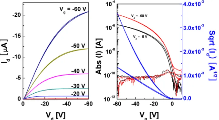
Inkjet printed P3HT FET devices showed good p-type characteristics, whose hole mobility was as high
as 0.1 cm2/Vs. As can be seen in Fig. 3, these P3HT
devices showed high on/off ratio more than 106, very
low gate leakage current, little contact resistance, and no significant bias hysteresis. It was commonly known that P3HT molecules are unstable in air ambient condition by photo-oxidation because of relatively low highest occupied molecular orbital (HOMO) energy level. However, top-gated and inkjet printed P3HT FETs in this study have shown little performance degradation after exposure to air, even P3HT was inkjet printed in air. The high air ambient stability was presumably due to self encapsulation effects of the top-gate dielectrics (low oxygen permeability of PMMA film).
Fig. 3. Output and transfer characteristics of inkjet printed P3HT FETs. (L = 20 µm / W = 1.0 mm)
For development of the polymeric complementary inverter circuits, where the combination of p- and n-channel transistors results in far greater circuit speeds, lower power dissipation and more stable operation,
0 -20 -40 -60 0 -5 -10 -15 -20 -20 V -30 V -40 V -50 V Id [ µ A ] Vd [V] Vg = -60 V
5-3 / K.-J. Baeg
IMID 2009 DIGEST •
high performance and easily printable both p- and n-channel polymer semiconductors must be developed. Polymeric complementary circuits are currently unrealized because of the absence of a suitable n-channel component. Recently, A. Facchetti et al. have discovered a high-performance, stable and readily processable electron-transporting polymeric
semiconductors, P(NDI2OD-T2).5
Fig. 4. Output and transfer characteristics of inkjet printed P(NDI2OD-T2) FETs. (L = 20 µm / W = 1.0 mm)
In this study, inkjet printed P(NDI2OD-T2) devices also showed very high performance of n-channel OFET characteristics, as shown in Fig. 4. We can obtained high electron mobility as high as 0.3 cm2/Vs using conventional PMMA gate dielectrics and proper selection of orthogonal solvents. Similar with those of P3HT FETs, P(NDI2OD-T2) transistors also showed high on/off ration, low threshold voltage, very low gate leakage current, little contact resistance and no significant bias hysteresis.
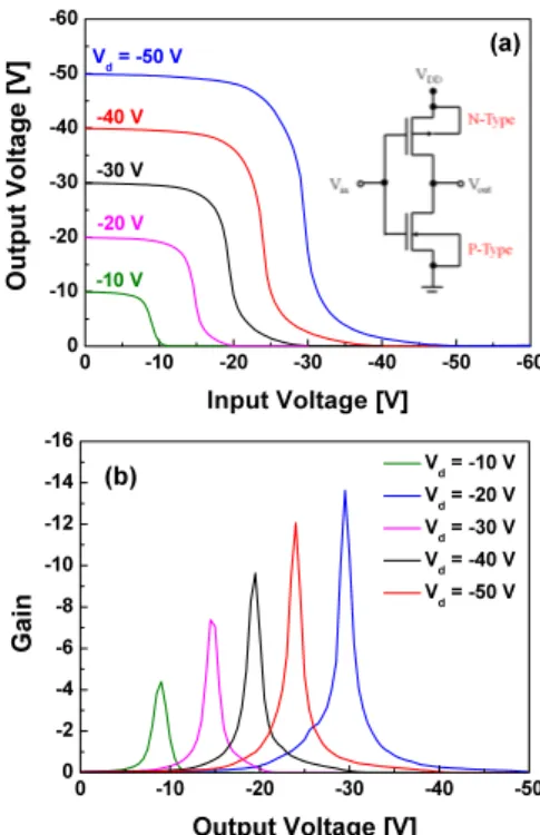
By appropriate combination of P3HT and P(NDI2OD-T2) transistors, we can demonstrated top-gated and inkjet printed polymeric complementary inverter circuit (with voltage gain 15) (Fig. 5). The inverter circuits were well operated at low operation voltage range as low as 10 V. Process optimization was still required and now in progress in our group to obtain more improved complementary polymer integrated circuits. We convinced that the proper combination of P(NDI2OD-T2) materials with previously developed high-performance p-channel polymers such as poly(3,3’''-dialkyl-quarterthiophene)s (PQT-12) and optimized device architectures will open unprecedented opportunities for printed electronics.5
0 -10 -20 -30 -40 -50 -60 0 -10 -20 -30 -40 -50 -60 -10 V -20 V -30 V -40 V O ut pu t V ol ta ge [V ] Input Voltage [V] Vd = -50 V (a)
Fig. 5. Inkjet printed complementary inverter circuits and inverter characteristics. .
4. Summary
High performance P3HT and P(NDI2OD-T2) top-gate/bottom-contact polymer field-effect transistors were fabricated using inkjet printing process and applied to elementary organic complementary inverter. We can obtain high electron and hole field-effect mobilities more than 0.1 cm2/Vs for both of p-channel and n-channel FETs, and successfully measured inkjet printed polymer inverter circuits.
Acknowledgement
This research was financially supported by development of next generation RFID technology for item level applications (2008-F052-01) funded by the
ministry of knowledge economy (MKE), the 2nd stage
Brain Korea 21 (BK21) program funded by the ministry of education, science and technology (MEST) of Korea, the national research laboratory (NRL) program of Korea science and engineering foundation (KOSEF), a grant (F0004021) from the information display R&D center one of the 21st century frontier R&D programs, the program for integrated molecular systems (PIMS) at GIST.
0 20 40 60 10-12 10-10 10-8 10-6 10-4 Vd = 5 V Vd = 60 V Vg [V] A bs (I ) [ A ] 0.0 2.0x10⁻³ 4.0x10⁻³ 6.0x10⁻³ 8.0x10⁻³ 1.0x10⁻² S qr t [ I d] [ A 1/2 ] 0 20 40 60 0 10 20 30 40 50 60 70 80 10 V Id [ µ A ] Vd [V] 20 V 30 V 40 V 50 V Vg = 60 V 0 -10 -20 -30 -40 -50 0 -2 -4 -6 -8 -10 -12 -14 -16 Vd = -10 V Vd = -20 V Vd = -30 V Vd = -40 V Vd = -50 V G ai n Output Voltage [V] (b)
5-3 / K.-J. Baeg
• IMID 2009 DIGEST
5. References
1. H. Sirringhaus, Adv. Mater., 17, 2411 (2005). 2. Y.-Y. Noh and H. Sirringhaus et al., Nature Nanotech., 2, 784 (2007).
3. E. Cantatore et al., IEEE Journal of Solid-State Circuits, 42, 84 (2007).
4. K.-J. Baeg and D.-Y. Kim et al., Adv. Mater., 18, 3179 (2006).