63-1 / S. G. Lee
• IMID 2009 DIGEST
Derivation of Current-Voltage Equation for OLED using Device Simulation
Sang Gun Lee*, Reiji Hattori
Dept. of Electronics, Kyushu University, Motooka, Nishi-ku, Fukuoka 819-0395, Japan
TEL: 81-92-583-7887, e-mail: [email protected]
Keywords: OLED, J-V characteristics, Theoretical equation, Verilog-A, Device simulation
Abstract
The theoretical equations for J-V characteristics in an OLED was derived according to the internal carrier emis-sion equation based on a diffuemis-sion model at Schottky bar-rier contact and the mobility equation based on the Pool-Frenkel model. The J-V characteristics of OLED are pre-sented using a behavioral model for analog systems (Ver-ilog-A language), and the accuracy of this model was veri-fied by comparing with the device simulation results.
1. Introduction
Unfortunately, the accurate current density-voltage (J-V) equation for organic light-emitting diode (OLED) has not been presented so far in textbooks and research pa-pers although the equation for inorganic semiconductor LED was presented clearly. One of the reasons is that the electrical transport characteristics in organic semicon-ductor is not revealed clear yet.
However, many OLED researchers are demanding the accurate theoretical equations of electrical transport which are possible to explain physical phenomena of OLED devices. Moreover, if theoretical equations are possible to describe the analog behavior model for OLED, the model is helpful for designing the compli-cated circuit including OLED such as the pixel circuit of active-matrix OLED (AMOLED). Therefore, clear defi-nition of the theoretical equation is strongly demanded. There are two way to derive theoretical equations of J-V characteristics. The general method is to derive from the experimental results. To confirm the validity in this method, the parameters of sample such as layer thickness, barrier height, or mobility have to be changed. But al-most all the parameters must be changed during the fab-rication process. In addition, it is also difficult to change these parameters individually because the fabrication parameters are closely related each other. The other method is to derive from the device simulation. This method is easy to change the individual parameters. Therefore, we derived the theoretical equations of J-V characteristics for OLED from the results calculated by the device simulation instead of experimental results. In addition, the J-V characteristics can present a behavioral model using Verilog-A language, and the accuracy of this model was verified by comparing with the device
simulation results.
The objectives in this work is to derive theoretical J-V equations in OLED for SPICE circuit simulation. In the previous work [1], we assumed that an electric field is just constant because of no space-charge effect, but we found that the field distribution had to be considered in case of low barrier height. Therefore, in this work, we extended the theoretical equations not only no space-charge effect but also space-space-charge effect, and we pre-sented the transition between injection limited and bulk limited current.
2. J-V equation for single layer unipolar device I. Injection limited current (JILC)
Generally, the thermionic emission model has been used to represent the injection current from the metal to the organic material through the Schottky barrier. This mechanism, however, is appropriate only in the semi-conductors with high mobility and long mean-free-path. In the case of organic semiconductors which have a low mobility and short mean-free-path, the injection current should obey a diffusion model [2]. Therefore we as-sumed that the injection current through Schottky barrier according to the diffusion model, which is given as fol-lows; exp B exp ILC q q J q EN E kT kT
φ
γ
µ
⎛ ⎞ ⎛ ⎞ = ⎜− ⎟ ⎜ ⎟ ⎝ ⎠ ⎝ ⎠ , (1)where q is an elemental charge, µ mobility, E electric field, N density of state, and φB injection barrier height.
The barrier lowering due to the image force is expressed by the last term with the factor, γ.
The mobility in the organic semiconductor usually has field dependence. Assuming the Coulomb potential of a charged trap, the mobility is expressed by the Pool-Frenkel model, which is given as follows;
0
exp
exp
a PFq
q
E
kT
kT
ε
β
µ
=
µ
⎛
⎜
−
⎞
⎟
⎛
⎜
⎞
⎟
⎝
⎠
⎝
⎠
, (2)mo-63-1 / S. G. Lee
IMID 2009 DIGEST • bility, εa the thermal activation energy of trapped carrier,
β the Poole-Frenkel factor as a fitting parameter. Substi-tuting this into Eq. (1) and assuming E=V/L over the whole layer, the following equation is obtained;
(
) (
)
0exp
a B ILCq
q
V
V
J
q N
L
kT
kT
L
ε φ
γ β
µ
⎡
+
+
⎤
=
⎢
−
+
⎥
⎣
⎦
, (3)This is the J-V equation for the injection limited cur-rent (JILC).
II. Bulk limited current (JBLC)
Figure 1 shows internal electric field distributions as a parameter of injection barrier height at 10 V in applied voltage, which were calculated by the device simulation. In the case of barrier height more than 0.2 eV, the elec-tric field is constant over the whole layer since the ade-quate amount of space charges is not generated yet. However, in case of barrier height lower than 0.1 eV, the electric field can’t be assumed to be constant anymore. Therefore, theoretical J-V characteristics must include the space-charge effect in case of low injection barrier height. 0.0E 0 5.0E 5 1.0E 6 1.5E 6 2.0E 6 2.5E 6 0 10 20 30 40 50 x (nm) E (V /c m ) Cathode Anode φB=0.2~0.5 eV φB=0.1 eV φB=0.05 eV φB=0.02 eV φB=0.01 eV
Calculated with Eq.(5)
Calculated with Eq.(4)
Fig.1. Internal electric field distribution for different injection
barrier height at 10 V in applied voltage.
The equation for electric field distribution including space-charge effect should be solved from the differen-tial equation according to dE dx= −qn ε εr 0 (Poisson’s equation) and J= −qn Eµ (continuity equation). If the mobility is independent of electric field, this equation is easily solved and well-known Mott-Gurney’s equation as follows;
(
)
20 0
2 BLC r
E= J µε ε x E+ , (4)
where εr is a relative permittivity, ε0 a vacuum
permittiv-ity and E0 the electric field at x=0 as an initial condition.
The dotted gray line in Fig. 1 is calculated by Eq. (4), which differs largely from the device simulation. The reason is because the mobility is assumed to be constant. On the other hand, in case of the mobility which has field-dependence as shown in Eq. (2), the following equ-ation is obtained [3];
(
3 3 2 2) ( )
0 0 0 42
3
6
6 exp
r BLCE
E
E
E
x x
J
µ ε ε β
β
β
β
β
−
+
−
= +
, (5)where the electric field, E, is varied with x, and x0 is
de-cided to E0 as an initial condition as follows;
(
3 3 2 2) ( )
0 0 0 4 0 0 0 02
3
6
6 exp
r BLCx
E
E
E
E
J
µ ε ε β
β
β
β
β
=
−
+
−
, (6)The dotted black line in Fig. 1 is calculated by Eq. (5), which can get a relatively good agreement with device simulation. In order to obtain the J-V relation, the Eq. (5) must be integrated again on x, but the equation gets too complicated to deal with. Therefore, if E is assumed to be very large under the condition at x=L, E0 and x0 can be
neglected, the approximate expression can be obtained as follows; 3 2 3 2 0 0 5 2
2
exp
r BLCV
V
J
L
L
µ ε ε α
β α
β
⎛
⎞
≈
⎜
⎜
⎟
⎟
⎝
⎠
, (7)where the E=α(V/L) is substituted into Eq. (5). The α is an adjusting parameter to fit E to the real value. This is the J-V equation for the bulk limited current (JBLC) with
field dependent mobility.
III. Transition between JILC and JBLC
We obtained the theoretical J-V equations (3) and (7), which are valid in different ends of conditions, that is, the JILC and JBLC, respectively. The J-V characteristics,
however, must be considered JILC and JBLC
simultane-ously. One of the simplest ways is that the total current density leads to equation as follows;
ILC BLC Total ILC BLC
J
J
J
J
J
⋅
=
+
, (8)This equation means that the current is simply limited by the smaller current, JILC or JBLC. This equation is not
derived from the accurate analysis but the transition be-tween the JILC and JBLC can be well expressed.
63-1 / S. G. Lee
• IMID 2009 DIGEST
Figure 2 shows J-V characteristics of single layer uni-polar device as a parameter of injection barrier height calculated from device simulation and theoretical equa-tion using Eq. (8). In both calculaequa-tions the same physical model and parameters were employed. As shown in Fig. 2, the both curves are completely overlapped, which means the theoretical equation can express the both cur-rents with a simple equation.
Fig. 2. Comparison of J-V characteristics in single-layer
uni-polar device between the results from device simulated and theoretically calculated.
Assuming the condition of JILC= JBLC, we can obtain
φBc as shown in Eq. (9), which means how low the
bar-rier height should be to obtain an ohmic contact. In other words, the barrier height does not have to be less than φBc. Notice that the mobility does not appear in this
equation, which means that the mobility has no effect on the contact characteristics. However, the φBc expressly
depends on device thickness and density of states in the device parameter. Therefore, the φBc is transited by
de-vice parameters as shown in Eq. (9).
(
)
{
}
3 2 02
1
ln
BckT
V
V
q
L
qNL
L
εε α
φ
β
α γ
β
⎡
⎛
⎞
⎤
=
⎢
−
+ −
⎜
⎜
⎟
⎟
⎥
⎢
⎝
⎠
⎥
⎣
⎦
, (9)3. J-V equation for double layer bipolar device
Figure 3 shows an energy diagram of double layer bi-polar device, that is the simplest OLED structure. The device is composed of an electron transport layer (ETL)
and hole transport layer (HTL) used in the simulation. The subscripts of e and h indicate the parameter for elec-tron and hole, respectively. The light emission occurs in ETL since the internal energy-band offset for electrons was assumed to be much higher than that for holes.
The J-V equation for double layer bipolar device is thought to be more complicated than that of single layer devices. There are many parameters related to the elec-tric conduction in the double layer bipolar device. All of them must be considered or included in the equation. However, we found that some of them can be neglected, and the J-V characteristics are obtained by considering the double layer device as two single layer devices con-nected in series. From previous work [1], we have re-vealed the important facts; (i) the electron-mobility in HTL, (ii) the hole-mobility in ETL and (iii) the internal energy-band offset for holes can be neglected in the J-V characteristics under the ordinary conditions.
Employing the above feature, the carrier balance can be achieved in the device, because the electrons are s-topped by the internal barrier, all holes recombine im-mediately near the interface in ETL, and no hole can reach to the cathode except the case of extreme low elec-tron mobility in ETL.
Bh qφ Be qφ e J − h J e µ h µ ETL HTL e L Lh h qV e h bi qV +qV +qV e qV
Fig.3. Energy diagram for double layer bipolar device.
When the carrier balance is achieved, the following equation is obtained;
e h
J
=
J
=
J
, (10)where Je and Jh are the current densities for electrons in
ETL and holes in HTL, respectively, and J is the total current density. Since the injected holes to ETL immedi-ately recombine in a narrow range near the interface un-der ordinal conditions, the space charge formed by holes has small effect on the electric field distribution. There-fore, each layer can be treated as a single layer device and its J-V characteristics are given by Eq. (8).
63-1 / S. G. Lee
IMID 2009 DIGEST •
The voltages applied to each layer are given by the following equation;
e bi h
V
=
V
+
V
+
V
, (11)where Vbi is a built-in potential corresponding to the
dif-ference between the work-functions of anode and cath-ode metals, V an applied voltage, and Ve and Vh voltages
applied on ETL and HTL, respectively. Solving Eq. (10) and Eq. (11) for ETL and HTL, simultaneously, J is de-cided uniquely by V, but they can not be solved in an algebraic manner. e V Vbi Vh e J Jh V
Fig.4. Equivalent circuit of double layer bipolar device.
In order to solve equations, we employed the equiva-lent circuit as shown in Fig. 4. Electrically, the single layer devices can be expressed as a diode and they are connected in series with the voltage source expressing the Vbi. Once the equation representing the relationship
between output and input are obtained, it is easy to gen-erate the analog behavior model using Verilog-A lan-guage. In addition, since the Verilog-A language can treat an internal node, it is possible to solve the simulta-neous equations even if the equations are not solved in an algebraic manner. The Verilog-A language is the computer programming language and an analogue ex-pansion of Verilog-HDL. Since the relation between J and V for the single layer device is already obtained in Eqs. (3), (7) and (8), we created the analog circuit model and calculated the J-V characteristics of double layer bipolar device according to the equivalent.
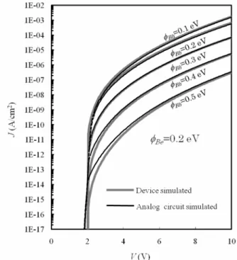
Figure 5 shows the results of J-V characteristics from the analog circuit simulation using the Verilog-A lan-guage as a parameter of Schottky barrier height for hole at anode comparing with that from the device simulation. The barrier height for electron at cathode (φBe) was fixed
at 0.2 eV. In both calculations the same physical model and parameters were employed. As shown in Fig. 5, good agreements between the device simulated and ana-log circuit simulated results were obtained expect for the cases of low voltage range. Similar to the single layer device, the J-V curves increase with decreasing the bar-rier height and the increase is discontinued less than 0.2
eV due to the JBLC. In the previous paper [1], we could
not include the space-charge effect, but it is successfully involved in this paper.
Fig. 5. Comparison of J-V characteristics in double-layer
OLED between the results from device simulated and analog circuit simulated.
4. Conclusions
We successfully derived theoretical J-V equations in single layer unipolar device and double layer bipolar device. These equations can successfully represent the transition between the injection limited current and bulk limited current. Using these equations, we described a SPICE model using Verilog-A language showing a good agreement with the results calculated from the device simulation.
5. Reference
[1] S. G. Lee and R. Hattori, IMID’08 Technical Digest, p. 431 (2008).
[2] S. M. Sez, Physics of Semiconductor Device, Wiley New York, 2nd edition, p. 254-270 (1981).
[3] P. N. Murgatroyd and H. H. Wills, J. PHYS.D: Appl. Phys., Vol. 3 151 (1970).