3-3 / W. S. Jeon
• IMID 2009 DIGEST
Abstract
We report simple structure red phosphorescent devices comprising only single organic layer structure. Maximum current efficiency of 9.44 cd/A and the driving voltage of 5.4 V are obtained in this single layer structure PHOLEDs, respectively. The mixed host system using electron transporting and hole transporting materials doped with Ir(piq)3
provides such high efficiency and reasonable driving voltage. The principal to simplification is the direct charges injection from the metallic electrodes into mixed host materials.
1. Introduction
The organic light emitting devices (OLEDs) have attracted considerable interest due to their potential application in low cost and high performance display and lighting [1]. Recently in the phosphorescent OLEDs (PHOLEDs), almost theoretical external quantum efficiency (EQEs) had been reported in several color devices [2~4]. Thermal evaporation technique and complicated fabrication process consisting of multiple layers for charge carriers balancing and exciton confinement are employed in highly efficient phosphorescent OLEDs. From the viewpoint of process, these complicated architectures should be improved if possible without losing the excellent performance. Many good approaches are enduring to reduce multiple organic layers until now. Several researchers have been achieved bi-layered devices with high efficiency.[5~7] Organic single layered PHOLEDs were recently reported by Z. Liu groups, their device performance was insufficient for the real application.[8]
In this study, we demonstrated high efficiency red PHOLEDs comprising only single organic layer. The key to the simplification is the direct injection of holes and electrons into mixed emitting host materials
through electrodes. Since the all charge carrier within OLEDs were injected from anode and cathode, performance and device structure are governed by metal/organic interfaces. In conventional OLEDs, the Fermi energy gap between cathode and surface treated anode is about 2.0~2.2 eV. This gap almost corresponds to red light energy. If the host materials has the proper HOMO and LUMO energy level, holes and electrons can be easily move from electrodes to emitting layer without any charge injection and transport layer for the red devices. However, these host materials are very rare. The mixed host system was an adequate method to solve lack of host materials. Mixed host system using hole transporting and electron transporting host materials already has been studied for the good charge balance. This system can match the energy levels between emitting host and electrodes as well as charge balance. In order to design single layer devices, hole type host material are required to have 5.1~5.4 eV HOMO energy levels matched with surface treated ITO Fermi level. Also, the 2.8~3.0 eV LUMO energy levels of electron transporting host materials are used to match the Fermi level of cathode. 4,4’,4”-Tris(N-3- methylphenyl-N-phenyl-amino)triphenylamine(m-MTDATA) and N,N’-diphenyl-N,N’-bis(1,1’-biphenyl)-4,4’-diamine (α-NPB) were used as the hole transporting host materials. Bis(10-hydroxybenzo[h]quinolinato)beryllium (Bebq2) with a
proper energy level was used as the electron transport host material. Tris[1-phenylisoqunolinato-C2,N]iridium (III) [Ir(piq)3] was employed as a red
phosphorescent guest.
2. Experimental
All organic materials were deposited by the vacuum evaporation technique under a pressure of ~ 3.0×10⁻⁷
Torr. Figure 1 shows the energy band-diagram of the
High Efficiency Red PHOLEDs with Organic Single Layer Structure
Woo Sik Jeon1, Tae Jin Park1, Jae Hyung Yu1, Ramchandra Pode2, Jin Jang1 and Jang Hyuk Kwon1*
1Dept. of Information Display and Department of Physics,
Kyung Hee University, Dongdaemoon-gu, Seoul 130-701, Korea TEL:82-2-961-0948, e-mail: [email protected]
3-3 / W. S. Jeon
IMID 2009 DIGEST •
single layer red PHOLEDs in this work. For the evaluation of single layer with different mixed host, the following devices were fabricated:
Device A: ITO/m-MTDATA:Bebq2:Ir(piq)3 [1~4 wt%,
100 nm]/LiF (0.5 nm)/Al (100 nm); Device B: ITO/α-NPB:Bebq2:Ir(piq)3 [1~4 wt%, 100
nm]/LiF (0.5 nm)/Al (100 nm).
The ratio of hole transporting and electron transporting hosts was fixed to 1:1. The doping concentrations were varied from 1% to 4% to optimize the device performance. The devices were fabricated on ITO coated glass with a sheet resistance of 20 Ω/□. The substrates were cleaned with acetone
and isopropyl alcohol sequentially, rinsed in de-ionized water, and then treated in UV-ozone immediately before loading into the high vacuum chamber (~ 2 × 10⁻⁷ Torr). The current density-voltage
(J–V) and luminance–voltage (L–V) data of red PHOLEDs were measured by Keithley 2635 A and Minolta CS-1000A, respectively. The red PHOLED emitting area was 6 mm2 for all the samples studied in
the present work.
Fig. 1. The energy band-diagram with different mixed host materials in organic single layer devices.
3. Results and discussion
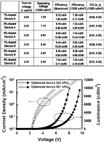
Table 1 shows the performance of red PHOLEDs devices comprising single emitting layer. The driving voltage (to reach 1000 cd/m2), maximum current and
power efficiencies values of 6.9 V, 8.04 cd/A, and 10.96 lm/W are reported in 4wt% doped device A, respectively. Very similar device performances are obtained in 2 wt% doped device A. We assume that 4% wt% doping is optimum condition because the highest efficiency is observed at general used brightness value (1000cd/m2). The driving voltage (to
reach 1000 cd/m2), maximum current and power
efficiencies values of 5.4 V, 9.44 cd/A, and 10.62 lm/W are reported in device B [1 wt%] as optimum doping condition, respectively. Maximum current efficiency for device A and B were appeared for the 4 wt%, 1 wt% of Ir(piq)3 doped mixed hosts,
respectively. The color coordinates are (0.66, 0.33) or (0.67, 0.32) for all devices. Even at 1% doped device, a good red color is observed. The results of device B [1wt %] is significantly superior to Ir(piq)3 doped
multi-layer red PHOLEDs.
Table 1. Summarized performance of single red device with various doping concentration.
Fig. 2. J-V-L characteristics of optimized single layer red PHOLEDs
The J-V-L characteristics of optimized device A and B appear in Figure 2. In these two devices, the driving voltage of device A using m-MTDATA:Bebq2 had
higher than that of device B with α-NPB:Bebq2 at the
1,000 cd/m2. Device A haven’t barrier for hole
injection from surface treated ITO to the HOMO of the m-MTDATA. Also, electrons can be easily injected from the cathode to LUMO of the Bebq2 in
device A. In the device B, the hole injection barrier of 0.3 eV between anode to mixed emitting layer exists,
3-3 / W. S. Jeon
• IMID 2009 DIGEST
while electrons easily injected from cathode to emitting layer. However, device B was driven lower voltage compare to device A. In order to find crucial factors to determine driving voltage, we fabricated undoped device without Ir(piq)3 dopant and J-V
characteristics were investigated.
Voltage (V) 0 2 4 6 8 10
Cu
rre
nt
De
ns
ity
(m
A/
cm
2)
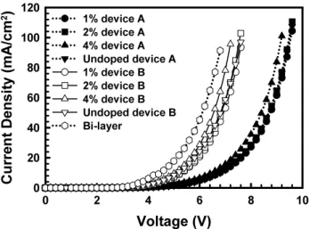
0 20 40 60 80 100 120 1% device A 2% device A 4% device A Undoped device A 1% device B 2% device B 4% device B Undoped device B Bi-layerFig. 3. J-V characteristics of device A, B with various doping concentration and bi-layered red devices.
Figure 3 shows J-V characteristics of device A, B with various doping concentration [0~4 wt%] and our previous reported bi-layered red device.[9] The current flows of undoped device A and B similar to doped device A and B. All mixed single layer device have a much slower current flows than bi-layered device with hetero junction. As shown in Figure 3, single layer devices almost don’t have serious charge trap dependence by dopant molecules and hole injection barrier at the ITO/mixed host interface is not so effective. Therefore we assume that charge mobility of m-MTDATA and α-NPB is an important parameter to determine driving voltage of our single layer devices. The interesting and intriguing J-V results in single layer host devices may be explained on the basis of existing knowledge of charge carrier mobility of in organic materials. α-NPB exhibits an ambipolar transporting ability with electron and hole mobility values of 9×10⁻⁴ and 6×10⁻⁴ ㎠/Vs, respectively, [10]
while the hole mobility value in m-MTDATA is 3×10⁻⁵
㎠/Vs. Earlier, it was shown that the charge transport
behaviors in mixed thin films of α-NPB and Alq3 are
sensitive to (i) compositional fraction, and (ii) charge mobility of neat compounds. The mixed layer appeared to have a lower mobility of charge carriers than neat films or bi-layer devices. [11] As a consequence, the
fast current flow in the device B despite of the large hole injection barrier is attributed to the high hole mobility value and ambipolar nature of α-NPB. Since the charge transport behaviors in mixed hosts are sensitive to the composition and intrinsic mobilities in neat films, a study of location of the recombination region may give us better understanding for our single layer devices.
Fig. 4. Luminescence-Efficiency characteristics of various single layer device with different locations of doped regions.
To investigate the recombination zone position, we have evaluated three devices with doped emissive layer located at different positions. If mixed layer mobility was sensitive, recombination regime may be changed from charge balance. Following devices are fabricated:
• Device A-(L) : ITO/m-MTDATA:Bebq2:Ir(piq)3 [4
wt%, 30 nm]/m-MTDATA:Bebq2 [70 nm]/LiF
(0.5 nm)/Al (100 nm);
• Device A-(C) : ITO/m-MTDATA:Bebq2 [35
nm]/m-MTDATA:Bebq2:Ir(piq)3 [4 wt%, 30
nm]/m-MTDATA:Bebq2 [35 nm]/LiF (0.5 nm)/Al
(100 nm);
• Device A-(R) : ITO/m-MTDATA:Bebq2 [30
nm]/m-MTDATA:Bebq2:Ir(piq)3 [4 wt%, 70
nm]/LiF (0.5 nm)/Al (100 nm).
Device B-(L), (C) and (R) were fabricated using α-NPB instead of m-MTDATA and 1 wt% of Ir(piq)3.
Doping region was fixed to 30 nm in all devices. Ir(piq)3 doped device A-(L) and B-(L) at the anode
side show best current efficiency as displayed in Figure 4. When doping region shifts to cathode, current efficiency gradually reduced. Mixed host system is the consequences of the better charge
3-3 / W. S. Jeon
IMID 2009 DIGEST •
balance in the recombination zone. The recombination zone for device A and B were located from center of device to slightly cathode side of center. Although holes are easily injected to organic layer in device A with m-MTDATA and Bebq2, the holes slowly
transported since m-MTDATA had a very low hole mobility and mobility decreased by mixed host, while electrons are rapidly transported by the Bebq2 in
device A and B. Thus, recombination zone located about center in device. Although holes are easily injected into the m-MTDATA/Bebq2 organic layer
(device A), they are slowly transported due to low hole mobility in m-MTDATA which is further reduced in the mixed host system. While transport behavior is relatively better in α-NPB/Bebq2 mixed host system
due to the high hole mobility in α-NPB. On the other hand, electrons are transported freely over the LUMO of the Bebq2 in doped devices A and B. These results
corroborate that the recombination zone in devices A and B are located between the center and anode regions of the emitting layer. The recombination zone in α-NPB/Bebq2 mixed host system are located to
more center side due to high mobility of α-NPB, which results higher device efficiency and lower driving voltage characteristics.
4. Summary
We demonstrate high efficiency red phosphorescent OLEDs comprising only single emitting layer. The key to the simplification is the direct injection of holes and electrons into the mixed host materials through electrodes. Maximum current efficiency of 9.44 cd/A and the driving voltage of 5.4 V are obtained in this single layer structure PHOLEDs, respectively. The principal to simplification is the direct charges injection from the metallic electrodes into mixed host materials. This is the first report on sublimated single layered PHOLEDs with a high efficiency and good driving voltage characteristics. The manufacturing process time of PHOLED devices also can be reduced by the simple structure architecture. The device characteristics of our single layer device are sufficient to apply to real display and lighting applications.
5. References
1. J. C. Scott, G. G. Malliaras, Chem. Phys. Lett., 299, 115(1999).
2. M. A. Baldo, S. R. Forrest, Phy. Rev. B, 62, 10958 (2000).
3. K. Coushi, R. Kwon, J. J. Brown, H. Sasabe, and C. Adachi, J. Appl. Phys. 95, 7798(2004).
4. D. Tanaka, H, Sasabe, Y.J. Li, S.-J. Su, T. Takeda, and J. Kido , Jpn. J. Appl. Phys. 2, Lett. (Japan), 46, L10 (2007).
5. W. S. Jeon, T. J. Park, S. Y. Kim, R. Pode, J. Jang, and J. H. Kwon, Appl. Phys. Lett, 93, 063303(2008).
6. J. Meyer, S. Hamwi, T. Bülow, H.-H. Johannes, T. Riedl, and W. Kowalsky, Appl. Phys. Lett, 91, 113506 (2007).
7. Z. W. Liu, M. G. Helander, Z. B. Wang, and Z. H. Lu, Appl. Phys. Lett, 94, 113305 (2009).
8. Z. Liu, M. G. Helander, Z. Wang, and Z. Lu, Organic Electron., 10, 1146 (2009)
9. T. J. Park, W. S. Jeon, J. J. Park, S. Y. Kim, Y. K. Lee, J. Jang, R. Pode, and J. H. Kwon, Appl. Phys. Lett. 92, 113308 (2008)
10. S. C. Tse, K. C. Kwok, and S. K. So, Appl. Phys. Lett. 89, 262102 (2006).
11. S. W. Liu, j. H. Lee, C. C. Lee, C. T. Chen, and J. K. Wang, Appl. Phys. Lett. 91, 142106 (2007).