P1-93 / J. W. Kwon
• IMID 2009 DIGEST
Abstract
We investigated the device performance for organic light-emitting characteristics based on the electron-injecting interfacial characteristics of Ba deposited on tris(8-quinolinolato)aluminum (III) (Alq3) with a change of a Ba coverage. The device performance of organic light-emitting diodes with Ba coverage of 1 nm significantly improved by the lowering of the electron-injecting barrier height that was induced by electronic charge transfer. However, the device with Ba coverage above 1 nm showed poor device performance. The spectroscopic results indicated that the Alq3 molecules started to decompose by the reaction between Ba and the phenoxide moiety of the molecule.
1. Introduction
The metal-organic interface has continuously been interested to improve the property for the carrier injection from electrodes to the organic layers such as a hole-injecting layer and an electron-injecting layer [1-3]. Among these interfacial metal-organic contacts, the electron-injecting barrier height [4-6] is generally larger than the hole-injecting barrier height in most of small organic molecules when each carrier is injected from electrodes to the organic layers. To improve the device performance, top-emitting OLEDs (TEOLEDs) with a Ba/Au cathode were fabricated with different thicknesses of Ba coverage (ΘBa) on Alq3 and their
electrical, optical, interfacial properties were investigated. In addition, the mechanism for the variation of device properties as a function of ΘBa on
Alq3 for the TEOLEDs was studied.
2. Experimental
The electronic structure of the Ba-on-Alq3
interfaces was examined by using x-ray photoemission spectroscopy (XPS) and ultraviolet
photoemission spectroscopy (UPS) at the 4B1 beam line in the Pohang Accelerator Laboratory (Korea). All measurements and depositions were performed in an ultra-high vacuum system, consisting of a main analysis chamber (approximately 5×10⁻¹⁰ Torr) and a
sample preparation chamber (approximately 5×10⁻⁹
Torr). All samples were prepared in situ by sequential thermal evaporation on a Si wafer and all thicknesses were determined by timed depositions calibrated using a quartz-crystal microbalance. In the XPS studies, incident photon energies of 650 and 550 eV were used to obtain the core level spectra of O 1s and N 1s, respectively. For the UPS measurements, the He I (21.2 eV) line from a UV source was used. The photoemission onset reflecting the vacuum level at the surface of all samples was measured by biasing the samples at -20 V. The incident photon energy was calibrated by measuring the Au 4f level of a clean Au surface.
The TEOLED was composed of glass / Ag (150 nm) / tin-doped indium oxide (ITO, 125 nm) / 4,4’,4”-tris(2-naphthylphenyl-1-phenylamino)triphenylamine (2-TNATA, 30 nm) / 4,4’-bis[N-(1-napthyl)-N-phenyl-amino]-biphenyl (NPB, 18 nm) / Alq3 (62 nm)
/ Ba / Au (20 nm), with ΘBa values of 0 nm (device 0),
1 nm (device 1), 2 nm (device 2), and 3 nm (device 3). All devices were fabricated by evaporation on glass / Ag / ITO substrates and the current density-voltageluminance characteristics were also measured using a Keithley 2400 electrometer, a photodiode (Oriel 71608), and a Keithley 485 picoammeter.
3. Results and discussion
When 1 nm-thick Ba was inserted between the cathode and Alq3,device 1 at the luminance of 100
cd/m2 (L
100) showed the highest power efficiency (ηPE)
Electronic Structure of the Tris(8-quinolinolato)aluminum
(III) (Alq
3) / Ba Interfaces and Light Out-coupling
Characteristics of Organic Light-emitting Diodes Based on
these Interfaces
JaeWook Kwon, JongTae Lim
and GeunYoung Yeom*
School of Advanced Materials Science and Engineering, Sungkyunkwan University, Suwon, Kyunggi-do 440-746, South Korea
P1-93 / J. W. Kwon
IMID 2009 DIGEST • of 2.3 lm/W. However, as ΘBa was increased to 2 and
3 nm, ηPE was reduced to 1.7 and 1.5 lm/W,
respectively. Those ηPE results indicate that the device
performance largely depends on ΘBa. The device
performance was maximized with 1 nm-thick ΘBa but
was deteriorated as ΘBa was increased above 1 nm.
To gain further insight on the mechanism involved in the device performance, electronic structures of the Ba-on-Alq3 interfaces were investigated as a function
of ΘBa.
Figure 1(a) shows the spectral region around the highest occupied molecular orbitals (HOMOs) of the Ba-on-Alq3 interfaces in the UPS spectra, as a
function of Ba ranging from 0 to 20 nm on Alq3. Also,
Fig. 1(b) in the UPS spectra shows the photoemission onset measured at the Ba-on-Alq3 interfaces as a
function of ΘBa ranging from 0 to 20 nm on Alq3 with
a sample bias of -20 V, reflecting the WF shifts of Alq3 achieved by Ba adsorption. In Fig. 1(a), all Alq3
molecular orbital features were shifted to a higher binding energy with increasing ΘBa.
Fig. 1. (a) The spectrum around the HOMO of the
Ba/Alq3 interfaces in the UPS spectra. (b) The
work function of Ba on Alq3. The values in the
figure are the Ba coverage.
The energy shift of the HOMO peak was maximized at ΘBa of 0.4 nm and the binding energy
remained approximately 0.4 eV higher than that of the pristine Alq3, as shown in Fig. 1(a). This lowering of
the HOMO levels indicates that an electron injection (ΦBN) is lowered as 0.4 eV when compared to that of
the pristine Alq3. In addition, as shown in Fig. 1(a),
the metal-induced gap state (MIGS), which is roughly a free-electron-like, [7] metal wave function penetrating into the organic semiconductor side, was observed at the forbidden energy gap of approximately 1.5 eV above the HOMO of Alq3. The
band between Alq3 and the cathode was realigned due
to the introduced MIGS and WF difference. [8] In fact, a new gap state has also been observed in several interfaces between a low WF metal (e.g., Li, Na, K, Ca, and Mg) and Alq3.[9]
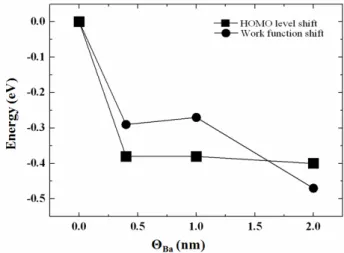
Figure 2 shows the WF shift (∆Ф=ФAlq3−Ф Ba-on-Alq3) from Fig. 1(a) and the HOMO level shift
(e0∆Vs=HOMOAlq3−HOMOBa-on-Alq3) from Fig. 1(b) as
a function of ΘBa ranging from 0 to 2 nm. The HOMO
level shifts can be expressed by e0∆Vs=∆I−∆Ф, where
∆I is the ionization energy change. The band bending (e0∆Vs) marked by the filled squares was not equal to
∆Ф(e0Vs ≠∆Ф) and the definite differences between e0
∆Vs and ∆Ф indicate that the HOMO-level shifts did
not simply originate from the WF difference but may have resulted from a possible chemical reaction between Alq3 and cathode.
Fig. 2. WF shift of ФAlq3−ФBa-on-Alq3 and the HOMO
level shift of HOMOAlq3−HOMOBa-on-Alq3 As a
function of ΘBa on Alq3 in the pristine Alq3 and
Ba-on-Alq3 interfaces.
We suggest that the lowering of this HOMO level is due not only to the band bending by Fermi level pinning, but also to the chemical modification of the Alq3 molecules by the excess electrons of the Ba
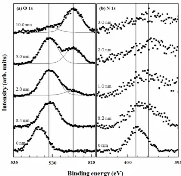
metal. Moreover, O 1s or N 1s spectra in X-ray photoemission spectroscopy (XPS) are evidence for the chemical reaction between Ba and Alq3 in Figure 3.
P1-93 / J. W. Kwon
• IMID 2009 DIGEST
Fig. 3. The evolution of XPS (a) O 1s, (b) N 1s core
level EDCs as a function of ΘBa on Alq3. The values
in the figures indicate ΘBa.
Figure 3 shows the evolution of the O 1s electron density curves (EDCs) as a function of ΘBa ranging
from 0 to 10 nm on Alq3 (10 nm), as measured by
XPS. For ΘBa=0 Å, the O 1s core-level electron
density curve (EDC) was symmetrical in shape and was composed of a single component, indicating a clean Alq3 film. The single component of the O 1s
EDC was initially shifted to a lower binding energy of 530.3 eV. Alq3 radical anion formed by electronic
charge transfer (ECT) from Ba until ΘBa= 0.4 nm,
compared with the pristine Alq3 of 531.6 eV. From
ΘBa= 2.0 nm, a O 1s peak of 527.3 eV (decomposition
by Al-O bond breaking) with low intensity began to appear at a lower binding energy, and the intensity of the 527.3-eV peak was further increased at ΘBa=5.0
nm. The peak shift to a lower binding energy was caused by a decrease in the Coulomb potential between the nuclei and the electrons of the valence band as a result of the increased electron density at the valence band of O atoms due to an electron provided by Ba
4. Summary
In summary, we investigated the mechanism of the improved device performance achieved by incorporating Ba in the cathode structure. At ΘBa of
1nm, the device performance was enhanced by the reduction of the HOMO level by about 0.4 eV. This reduction was due to band bending formed by Fermi level pinning as well as chemical reaction between Ba and Alq3. Although the ΦBN values at ΘBa of 0.4 and
2.0 nm were almost identical, the interface chemistry largely depended on ΘBa. The formation of a stable
radical anion at ΘBa= 0.4 nm enhanced the device
performance of the TEOLED but the appearance of a metallic component from ΘBa= 2.0 nm degraded the
device
5. References
[1] G. W. Scherer, J. Am. Ceram. Soc., 1990, 73[11], 3. [2] H. J. Kim and J. S. Im, SID’05 Technical Digest,
2005, Vol. 1, p.401.
[3] O. V. Mazurin and E. A. Porai-Koshits (eds.),
Phase Separation in Glass, North-Holland,
Amsterdam, 1984, p.21.
[4] D. L. Eaten, Porous Glass Support Material, US
Patent. 1975, no. 904, 422.
[5] K. D. Hong, IMID’06 Technical Digest, 2006, p.877.
[6] J. T. Lim, G. Y. Yeom, K. Lhm, and T.-H. Kang, J.
Appl. Phys. 2009, 105, 083705.
[7] M. Kiguchi, R. Arita, G. Yoshikawa, Y. Tanida, S. Ikeda, S. Entani, I. Nakai, H. Kondoh, K. Saiki, and H. Aoki, Phys. Rev. B 2005, 72, 075446. [8] J. Tersoff, Phys. Rev. Lett. 1984, 52, 465..
[9] C. Shen, I. G. Hill, A. Kahn, and I. Schwartz, J.