Optical characteristics of YVO
4
:Eu
3+
phosphor
in close proximity to Ag nanofilm: emitting layer
for mirror-type displays
Cheol Jang, Seong Min Lee, and Kyung Cheol Choi*Department of Electrical Engineering, KAIST, Yuseong-gu, Daejeon 305-701, South Korea
Abstract: We demonstrate the optical characteristics of YVO4:Eu 3+
phosphor in close proximity to Ag nanofilm to create a highly efficient emitting layer in mirror-type self-emissive displays. The propagating surface plasmon mode induced between the dielectric layer (MgO) and the Ag nanofilm activates the electric dipole transition of Eu3+ ions. The transmittance of a 100 nm-thick Ag nanofilm is zero in the visible wavelength range, making this nanofilm a good reflector in the visible wavelength range and capable of fulfilling a mirror function. The emission of an YVO4:Eu3+ phosphor layer with a 100 nm-thick Ag nanofilm was
enhanced to the point that it was eight times higher than that of a reference sample without Ag nanofilm. Therefore, the present work shows potential for application to mirror-type displays with high luminous efficacy.
©2012 Optical Society of America
OCIS codes: (250.5403) Plasmonics, (250.5230) Photoluminescence, (160.5690)
Rare-earth-doped materials.
References and links
1. G. Gu, Z. Shen, P. E. Burrows, and S. R. Forrest, “Transparent flexible organic light‐emitting devices,” Adv. Mater. (Deerfield Beach Fla.) 9(9), 725–728 (1997).
2. P. Görrn, M. Sander, J. Meyer, M. Kröger, E. Becker, H. H. Johannes, W. Kowalsky, and T. Riedl, “Towards See‐Through Displays: Fully Transparent Thin‐Film Transistors Driving Transparent Organic Light‐Emitting Diodes,” Adv. Mater. (Deerfield Beach Fla.) 18(6), 738–741 (2006).
3. J. F. Wager, “Applied physics. Transparent electronics,” Science 300(5623), 1245–1246 (2003).
4. S. R. Forrest, “The path to ubiquitous and low-cost organic electronic appliances on plastic,” Nature 428(6986), 911–918 (2004).
5. G. Gu, P. E. Burrows, S. Venkatesh, S. R. Forrest, and M. E. Thompson, “Vacuum-deposited, nonpolymeric flexible organic light-emitting devices,” Opt. Lett. 22(3), 172–174 (1997).
6. Y. Chen, J. Au, P. Kazlas, A. Ritenour, H. Gates, and M. McCreary, “Electronic paper: Flexible active-matrix electronic ink display,” Nature 423(6936), 136 (2003).
7. S.-M. Lee, S. H. Oh, and K. C. Choi, “Highly Transparent SU-8 Photoresist Barrier Rib for a Transparent AC Plasma Display Panel,” IEEE/OSA Journal of Display Technology 7(1), 40–43 (2011).
8. K. Aslan, Z. Leonenko, J. R. Lakowicz, and C. D. Geddes, “Annealed silver-island films for applications in metal-enhanced fluorescence: interpretation in terms of radiating plasmons,” J. Fluoresc. 15(5), 643–654 (2005). 9. N. Noginova, Y. Barnakov, H. Li, and M. A. Noginov, “Effect of metallic surface on electric dipole and
magnetic dipole emission transitions in Eu3+ doped polymeric film,” Opt. Express 17(13), 10767–10772 (2009). 10. K. Okamoto, I. Niki, A. Shvartser, Y. Narukawa, T. Mukai, and A. Scherer, “Surface plasmon enhanced super
bright InGaN light emitter,” Phys. Status Solidi 2(7), 2841–2844 (2005).
11. P. B. Johnson and R. W. Christy, “Optical Constants of the Noble Metals,” Phys. Rev. B 6(12), 4370–4379 (1972).
12. S. M. Lee, K. C. Choi, D. H. Kim, and D. Y. Jeon, “Localized surface plasmon enhanced cathodoluminescence from Eu3+-doped phosphor near the nanoscaled silver particles,” Opt. Express 19(14), 13209–13217 (2011). 13. S. M. Lee and K. C. Choi, “Enhanced emission from BaMgAl10O17:Eu2+ by localized surface plasmon resonance
of silver particles,” Opt. Express 18(12), 12144–12152 (2010).
14. A. K. Levine and F. C. Palilla, “A new, highly efficient red-emitting cathodoluminescent phosphor (YVO4:Eu) for color television,” Appl. Phys. Lett. 5(6), 118 (1964).
15. G. Blasse, A. Bril, and W. C. Nieuwpoort, “On the Eu3+ fluorescence in mixed metal oxides: Part I-The crystal structure sensitivity of thr intensity ratio of electric and magnetic dipole emission,” J. Phys. Chem. Solids 27(10), 1587–1592 (1966).
16. J. H. Kang, M. Nazarov, W. B. Im, J. Y. Kim, and D. Y. Jeon, “Characterization of nano-size YVO4:Eu and (Y,Gd)VO4:Eu phosphors by low voltage cathodo- and photoluminescence,” J. Vac. Sci. Technol. B 23(2), 843– 848 (2005).
17. A. F. Kirby, D. Foster, and F. S. Richardson, “Comparison of 7F
J←5DO emission spectra for Eu (III) in crystalline environments of octahedral, near-octahedral, and trigonal symmetry,” Chem. Phys. Lett. 95(6), 507– 512 (1983).
18. C. D. Geddes and J. R. Lakowicz, “Editorial: Metal-enhanced fluorescence,” J. Fluoresc. 12(2), 121–129 (2002).
1. Introduction
Recently, various noble displays, such as transparent displays [1–3] and flexible displays [4– 6], have been developed based on conventional flat-panel display platforms. These noble displays allow more freedom in the design of electronic devices. Thus, it is expected that their use will open a new market heralding the replacement of pre-existing components. In the same manner, mirror-type displays are a viable candidate for future displays. Mirrors are common in our everyday life. Mirror-type displays can be widely used in applications requiring the function of a both mirror and a display device simultaneously. A mirror-type display can be fabricated by placing a transparent display device in front of a perfect reflector. Transparent display devices based on AC plasma displays are superior candidates for mirror-type displays due to their simple structure [7]. AC plasma displays do not require thin-film transistors for operation, in contrast to other display platforms, such as organic light-emitting diodes and liquid-crystal displays, which do require these components. Thus, mirror-type displays using transparent AC plasma displays have the advantages of large-scale feasibility and easy fabrication. To develop a transparent AC plasma display, a metal film reflecting visible light must be attached to the back side of a transparent AC plasma display. Moreover, all of the components must be fabricated from transparent materials, including the inorganic phosphor.
Because the use of a transparent inorganic phosphor involves a tradeoff between thickness and photoluminescence, a transparent inorganic phosphor of nanoscale thickness has a performance issue. Therefore, a breakthrough is required to address this low luminescence issue. To achieve this aim, we propose a mirror display structure that uses Ag nanofilm as a reflector. Previous research has shown that propagating surface plasmons originating from metallic film can enhance the fluorescence and phosphorescence from semiconductors, organic molecules, and rare-earth ion complexes [8–10]. In this paper, we propose a phosphor layer structure as a component of a mirror-type AC plasma display in which Ag nanofilm functioning as a reflector is located near the phosphor layer. The proposed structure can reflect most of the visible light and the luminescence of transparent phosphor can be intensified by the propagating surface plasmon resonance due to the Ag nanofilm.
2. Experimental
Figure 1(a) shows the proposed emitting layer structure for a mirror-type display. Because mirror-type displays must reflect visible light when their display cells are turned off, all of the components above the reflector must be transparent. Thus, the proposed structure consists of a transparent phosphor layer (top), a dielectric layer (MgO), metallic nanofilm (Ag), and an indium tin oxide (ITO)-coated glass substrate. First, Ag nanofilms were thermally evaporated onto ITO-coated glass substrates. Considering the reflectivity, the Ag nanofilms were deposited from 0 nm to 150 nm. A 20 nm-thick MgO dielectric layer was deposited on the Ag nanofilm using the e-beam evaporation method. Propagating surface plasmons are then induced along the border between the MgO layer and the Ag nanofilm. A 100 nm-thick transparent phosphor layer (YVO4:Eu3+) was deposited by means of RF magnetron sputtering
at 150°C. The doping concentration of the Eu was 5%. The deposition thickness was monitored using a quartz crystal oscillator. The surface morphologies of the evaporated Ag nanofilms were determined via scanning electron microscopy (SEM) with a FEI (Netherlands) Sirion microscope. The transmittance of the fabricated samples was collected by a Shimadzu spectrophotometer (UV-2550, Japan). The emission spectra of the phosphors were acquired by a Hitachi spectrophotometer (F-7000, Japan). Also, the decay times of the phosphors were
measured by a time-resolved photoluminescence system composed of a flash Xe lamp (PSI corp., Korea) and a Tektronix oscilloscope (DPO3014, USA). In this case, the emission spectrum and the decay time from the phosphor were evaluated under the illumination of a continuous wave light and pulsed wave light operating at 254 nm UV, respectively.
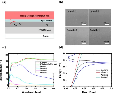
Glass MgO(20 nm) Ag Transparent phosphor(100 nm) ITO(150 nm) (c) 300 400 500 600 700 800 0 20 40 60 80 100 T r a n sm it ta n c e[ % ] Wavelength[nm] ITO glass ITO glass/MgO(20 nm) Sample 1 Sample 2 Sample 3 Sample 4 (d) (a) Ksp 0.00 0.02 0.04 0.06 0.08 0.10 1.5 2.0 2.5 3.0 3.5 4.0 E n er g y [ eV ] Ksp [1/nm] Ag/SiO2 Au/SiO2 Ag/MgO Au/MgO Sample 1 Sample 2 Sample 3 Sample 4 200 nm 200 nm 200 nm 200 nm (b)
Fig. 1. (a) Graphical representation of the emitting layer with a localized surface plasmonic structure containing Ag nano-films, (b) SEM images of Ag nanofilm deposited on the ITO-coated glass; the scale bar is 200 nm. (c) Transmittance of fully fabricated structures in a visible range, (d) energy dispersion curve versus the K vector of Ag films and Au films in various dielectric mediums; dielectric mediums are examined by MgO and SiO2.
Figure 1(b) shows SEM images of Ag nanofilms deposited onto ITO-coated glass substrates. The thicknesses of the Ag nanofilms of samples 1, 2, 3, and 4 were 20 nm, 50 nm, 100 nm, and 150 nm, respectively. The grain size increased as the thickness of the Ag nanofilms increased, resulting in a lowering of the transmittance. Figure 1(c) shows the transmittance measured from the fabricated samples. While samples 1 and 2 remained transparent at short wavelengths, the transmittances of samples 3 and 4 were zero across the entire visible wavelength. This result indicates that the film must be 100 nm thick for it to function as a perfect reflector. Ag and Au are known to be transition metals for surface plasmon resonance in the visible range. In fact, Au may be feasible for plasmon-resonance with red-emitting materials. However, an MgO dielectric layer with a high refractive index enables the plasmon resonance of Ag to be shifted toward the red emission wavelength, as shown in Fig. 1(d). The energy dispersion between the metallic film and the dielectric layer was theoretically calculated from the optical constant introduced by Johns and Christy [11]. The relative dielectric constant of MgO was collected by means of a Woollam spectroscopic ellipsometer (M2000D RCT, USA). In this work, we choose Ag nanofilm as a metallic reflector, as it is more cost-effective than Au nanofilm.
3. Results and discussion: PL spectra of phosphor on Ag films
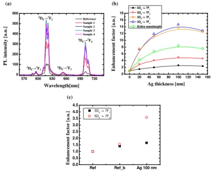
Figure 2(a) shows the photoluminescence (PL) intensity from the YVO4:Eu 3+
phosphor in close proximity to Ag nanofilms. In general, YVO4:Eu3+ phosphor has four radiative
emissions: 5D0→ 7 F1 (590 nm peak), 5 D0→ 7 F2 (618 nm peak), 5 D0→ 7 F3 (650 nm peak), and
5
D0→7F4 (700 nm peak). The radiative transition emission at 590 nm is magnetic-dipole-like
emission, while the other types are electric-dipole-like [12,13]. As shown in Fig. 2(a), samples having a phosphor/dielectric/Ag nanofilm structure show enhanced emission intensity compared to the reference sample without Ag nanofilm. Figure 2(b) shows the enhancement factors of the integrated PL intensity compared to that of the reference sample. To calculate the enhancement factors, the integrated PL intensity of the samples with Ag nanofilms was divided by the integrated intensity of the reference sample without Ag nanofilm. As a result, the PL intensity integrated over the entire region was enhanced nearly eight-fold relative to the original reading. It is remarkable that the emission intensities of the electric-dipole transition were visibly enhanced. The emission intensities around the peaks governed by the electric dipole transition show a considerable increase, while the emission intensity around 590 nm as governed by the magnetic dipole transition showed only a slight increase. The enhancement factor is maximized at the fourth radiative transition. Also, the enhancement in all of the samples became saturated after the Ag nanofilm reached a thickness of 100 nm. To distinguish the enhancement caused by the reflection of the Ag nanofilm from that caused by the propagating surface plasmon resonance, we carried out a photoluminescence measurement after attaching a metallic reflector onto the backside of the samples. This result is shown in Fig. 2 (c). When a metallic plate for reflection was attached to the backside of the reference sample, as shown in Fig. 2 (c) labeled as “Ref_b,” the magnetic dipole and electric dipole transitions of the phosphor layer both increased until they were 1.5 times higher than that measured without the metallic plate. However, in the case of sample 3, with a 100 nm-thick Ag nanofilm, the emission of the electric dipole transition was increased to a much greater extent than that of the magnetic dipole transition, even when the metallic reflector was present. Considering these results, we concluded that the increased emission from the phosphor layer is not due to the reflection caused by the operation of the mirror but is caused by the propagating surface plasmon-induced luminescence. For a better understanding of this phenomenon, we measured the time-resolved photoluminescence in an effort to prove the existence of the propagating surface plasmon.
570 600 630 660 690 720 0 100 200 300 400 500 600 P L i n te n si ty [ a .u .] Wavelength[nm] Reference Sample 1 Sample 2 Sample 3 Sample 4 (a) (b) 5D0→7F1 5D0→7F2 5D 0→7F3 5D 0→7F4 0 20 40 60 80 100 120 140 160 0 2 4 6 8 10 12 14 16 18 E n h a n c em en t fa ct o r [a .u .] Ag thickness [nm] 5D0 -> 7F1 5D0 -> 7F2 5D0 -> 7F3 5D0 -> 7F4 Entire wavelength Ref Ref_b Ag 100 nm 0.0 0.5 1.0 1.5 2.0 2.5 3.0 3.5 4.0 4.5 5D 0 -> 7F1 5D 0 -> 7F2 E n h a n ce m en t fa ct o r [a .u .] (c)
Fig. 2. (a) Photoluminescence intensity from the emitting layer with the propagating surface plasmonic structure incorporating Ag nanofilms, (b) enhancement factor calculated by dividing the integrated intensity of the sample with Ag films by that of the reference sample without Ag film
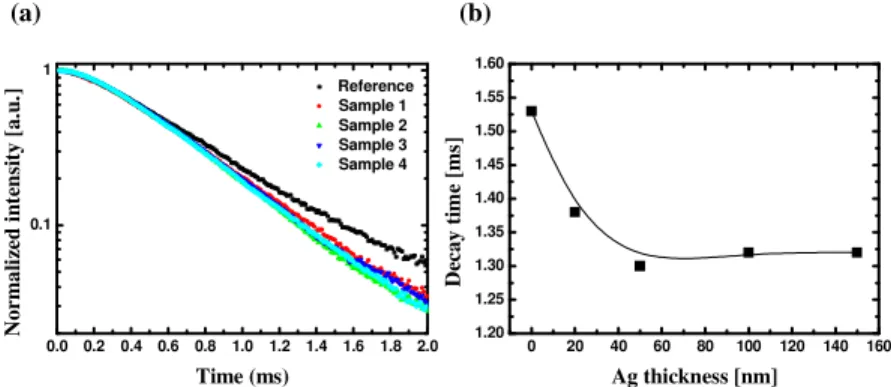
Figure 3 shows the time-resolved photoluminescence results and the estimated decay time of each sample. Time-resolved photoluminescence was carried out using a pulsed Xe lamp at room temperature (300 K). An oscilloscope was connected to the photoluminescence measurement system to observe the decay of the emission intensity. In Fig. 3(a), the photoluminescence intensities were normalized by the maximum value of each sample. The decay of the samples with Ag nanofilm was faster than that of the reference sample without Ag nanofilm. Figure 3(b) shows the decay time of the samples. The decay time (τ) is the time required for the emission intensity to be reduced to 1/10 of its initial value [14]. While the decay time of the reference sample was 1.53 ms, those of samples 1 and 2 were 1.37 ms and 1.30 ms, respectively. As the thickness of the Ag nanofilm increases, the decay time is reduced until it finally becomes saturated.
0 20 40 60 80 100 120 140 160 1.20 1.25 1.30 1.35 1.40 1.45 1.50 1.55 1.60 D ec a y t im e [m s] Ag thickness [nm] 0.0 0.2 0.4 0.6 0.8 1.0 1.2 1.4 1.6 1.8 2.0 0.1 1 N o rm a li ze d i n te n si ty [ a .u .] Time (ms) Reference Sample 1 Sample 2 Sample 3 Sample 4 (a) (b)
Fig. 3. (a) Decay time measurement of the emitting layer in close proximity to Ag nanofilm. For clarity, the decay curves are plotted using the logarithm (base 10). (b) Decay time estimated until the initial intensity decreased below a level of 1/10.
We demonstrated a phosphor structure that functions as a mirror via coupling with propagating surface plasmons of Ag nanofilm. We also elucidated the mechanism by which propagating surface plasmons can be used to enhance the luminescence from Eu3+-doped phosphor layers. As shown in the emission spectrum, the Eu3+-doped inorganic phosphor shows a number of radiative transitions arising from the initial 5D0 state to the final 7Fn (n = 1,
2, 3, 4) manifolds [15,16]. According to a previous theory [17], the first radiation peak (5D0
→7F1) is predicted to be primarily the magnetic dipole transition. The 5D0 → 7F2,4 transitions are allowed by the electric dipole transition. The 5D0 → 7F3 transition is predicted to be
summed by the (first-order) magnetic dipole and the (second-order) electric dipole transition. While the magnetic dipole transition is non-sensitive to the charge distribution and the site-asymmetry around the Eu3+ ion, the electric dipole transition is hypersensitive to the charge distribution and site-asymmetry, which can be modified by the localized and propagating surface plasmon resonance due to the metallic structure. Therefore, we believe that Ag nanofilm inserted as a reflector can enhance the luminescence by means of resonant coupling between the propagating surface plasmons and the electric dipole transition of phosphor materials. Although the 5D0 → 7F1 transition, governed primarily by the magnetic dipole,
seldom increased apart from the increase caused by the mirror reflection, the 5D0 → 7F3
transition by the (second-order) electric dipole could be enhanced in the same manner as the other electric dipole allowed transitions. As the thickness of the Ag nanofilm increased, the decay time of the luminescence intensity decreased and then remained constant past a thickness of 50 nm. This trend corresponds to the aspect of luminescence. The decrease in the decay time and the increase in the luminescence intensity become saturated when the thickness of the Ag nanofilm exceeds 50 nm. The following equations explain how metal plasmons can modify the intrinsic quantum efficiency and intrinsic decay time [8,18]:
0 0 1 , . nr nr Q k k τ Γ = = Γ + Γ + (1) 1 , . m m m m nr m nr Q k k τ Γ + Γ = = Γ + Γ + Γ + Γ + (2)
In Eqs. (1) and 2, Q0 and Qm are the intrinsic and modified quantum efficiencies,
respectively. Here, Г and knr are the radiative and non-radiative decay rates, respectively.
Also, Гm is the metal-induced radiative decay rate. In addition, τ0 and τm refer to the intrinsic
and metal-modified decay time. The decreased decay time and increased luminescence in our results are clearly explained by the modified equations. When a light emitter is coupled with surface plasmons owing to the metallic structure, a new radiation transition path will be introduced. That is, the newly induced term knr causes the quantum efficiency to be increased
and the decay time to be decreased. The radiative transitions by the electric dipole can be enhanced by the propagating surface plasmons due to the Ag/dielectric surface. As a result, the Ag nanofilm applied in the proposed structure can enhance the luminescence of rare-earth-doped phosphor.
4. Conclusion
In summary, we elucidated the optical characteristics of YVO4:Eu3+ phosphor in close
proximity to nanoscale Ag film when excited by UV light. The proposed structure has a dielectric layer for a nano-gap between the phosphor and a metallic reflector. Propagating surface plasmons can be generated at the border of the dielectric layer (MgO) and the Ag nanofilm. The plasmons can enhance the luminescence from YVO4:Eu3+ by stimulating an
electric dipole transition of Eu3+ ions. Because Ag nanofilms can function as a reflector, we believe that the proposed structure has a strong potential for application to mirror-type displays with high luminous efficacy.
Acknowledgments
This research was supported by the Basic Science Research Program through the National Research Foundation of Korea (NRF) funded by the Ministry of Education, Science, and Technology (CAFDC-20100009890). This research was also supported by a grant (F0004072-2010-33) from Information Display R&D Center, one of the Knowledge Economy Frontier R&D Programs funded by the Ministry of Knowledge Economy of the Korean government.